Solar cell peparation method

a solar cell and peparation method technology, applied in the direction of sustainable manufacturing/processing, climate sustainability, semiconductor devices, etc., can solve the problems of electricity not being allowed to pass between the upper and lower portions of the solar cell, the technique of separating a compound semiconductor from the substrate in the process of fabricating a solar cell semiconductor device has become an issue, and it is impossible to form an electrode on the bottom surface of the micro device, etc., to achieve the effect of high unit pri

Inactive Publication Date: 2018-11-15
GWANGJU INST OF SCI & TECH
View PDF5 Cites 1 Cited by
  • Summary
  • Abstract
  • Description
  • Claims
  • Application Information

AI Technical Summary

Benefits of technology

[0022]The method for fabricating the solar cell according to the present invention may have advantages in that the device is transferred to the flexible substrate without using the adhesive in the transfer printing process of separating the semiconductor device from the semiconductor substrate, thereby fabricating the vertical-type solar cell.
[0023]In the method for fabricating the solar cell according to the present invention, since the transfer printing process is performed after separating the epitaxially grown compound semiconductor solar cell from the compound semiconductor substrate having the relatively high unit price, the substrate may be recycled, and the separated thin film-type devices may be used for fabricating the flexible electronic devices.

Problems solved by technology

In addition, the solar cell is attracting attention as an energy source that supplies energy to areas where establishment of power plants are difficult because of relatively small geographical limitations.
A technique for separating a compound semiconductor from a substrate in a process of fabricating a solar cell semiconductor device has become an issue.
However, since the adhesive used for the transfer onto the flexible substrate is an insulation material, electricity is not allowed to pass between upper and lower portions.
As a result, it is impossible to form an electrode on a bottom surface of the micro device.
The vertical structure may not be used in fabricating a thin film solar cell using the transfer printing process due to the problem of the adhesive in the transfer printing process.
In addition, in the process of forming a bottom electrode facing a top surface, when the bottom electrode is formed to have a thin thickness, it may be difficult to perform an etch stop in a bottom contact layer, and the bottom electrode may be broken during to the transfer printing.
Thus, there is a problem that the bottom contact layer becomes thick.
When the bottom contact layer is formed to have the thick thickness, fabricating costs increase, and strain increases in proportion to the thickness to deteriorate the flexibility of the fabricated solar cell device.

Method used


Image

  • Solar cell peparation method
  • Solar cell peparation method
  • Solar cell peparation method

Examples


Embodiment Construction

[0027]Although embodiments are described in detail with reference to the accompanying drawings, the present invention is not limited to the embodiments. Moreover, detailed descriptions related to well-known functions or configurations will be ruled out in order not to unnecessarily obscure subject matters of the present invention.

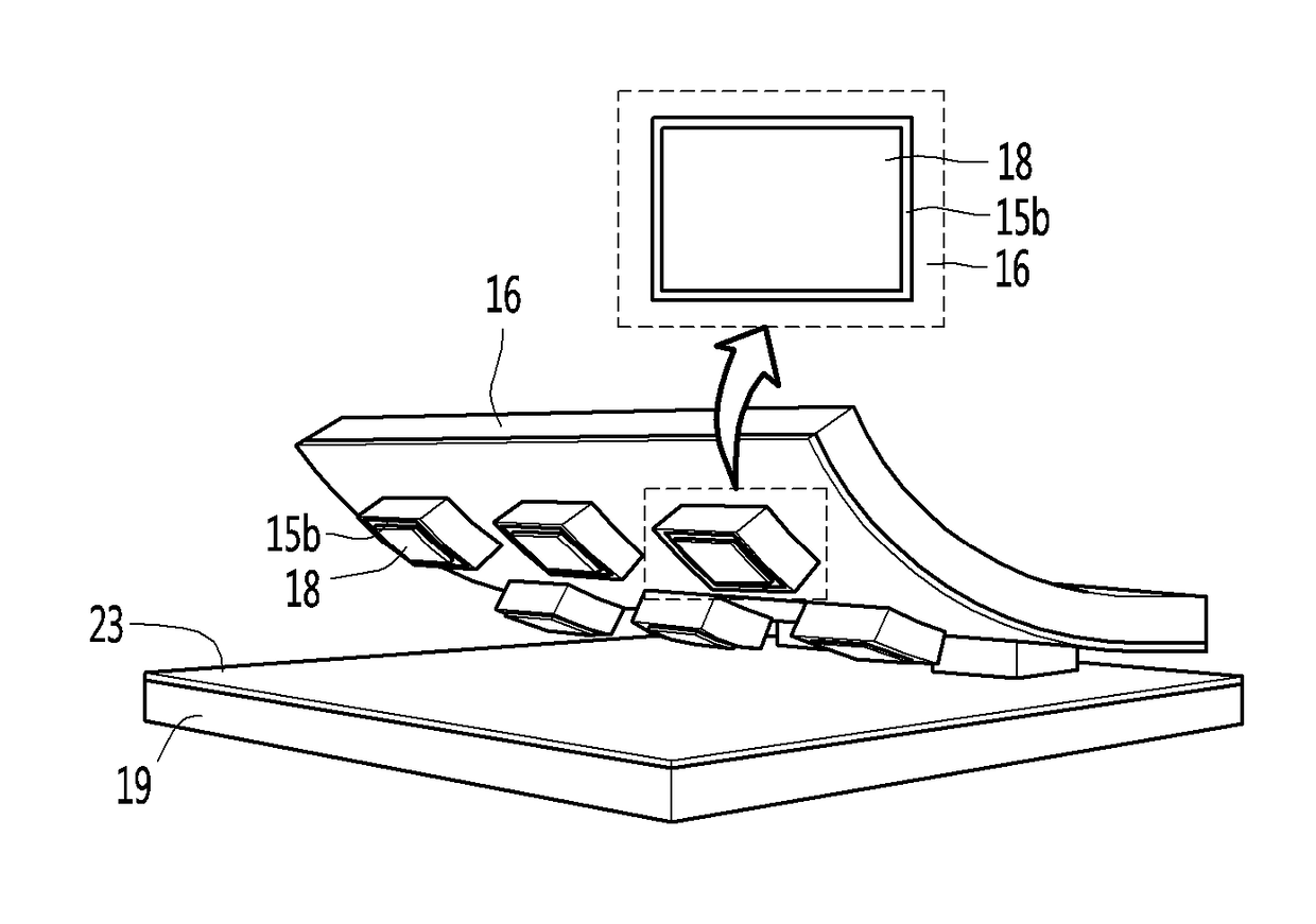
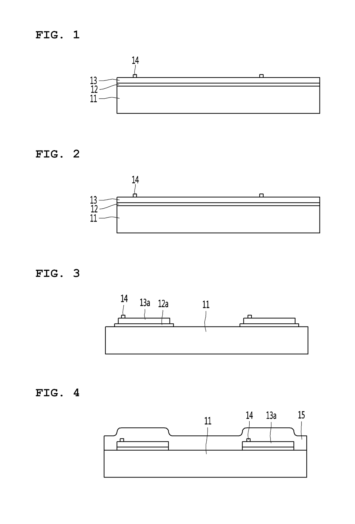
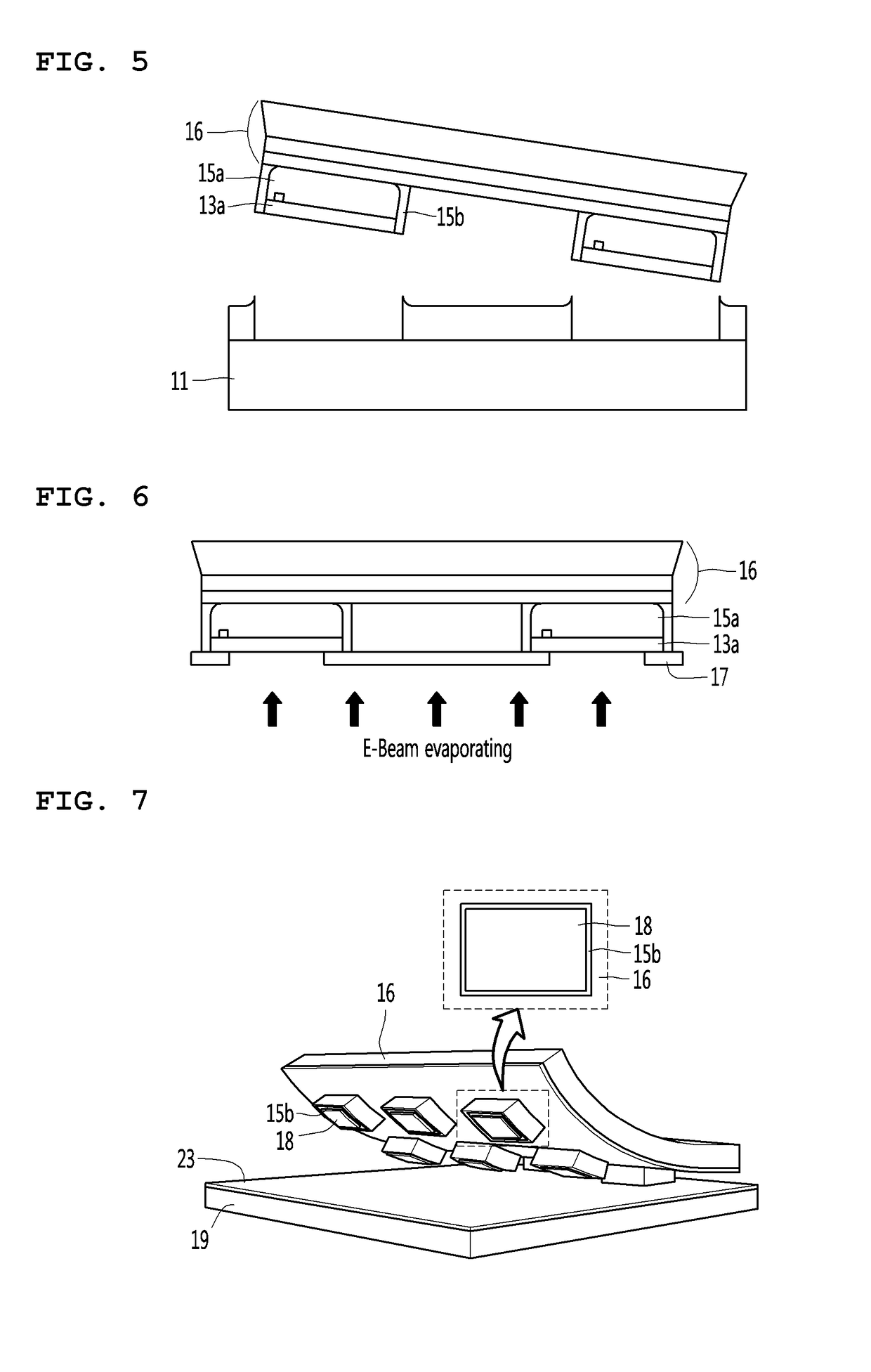
[0028]FIGS. 1 to 6 are views illustrating a process of preparing a micro device sample to be transferred in a method for fabricating a solar cell according to an embodiment. A process of preparing a micro device sample to be transferred may include a step of preparing a substrate including a sacrificial layer to pattern a solar cell layer and a top electrode on a top surface, a step of patterning the sacrificial layer so that the sacrificial layer has a surface area greater than that of the solar cell layer, a step of applying photoresist to an upper portion of the substrate and performing an undercut process on the sacrificial layer, a step of attaching a ...


PUM


Abstract

A method for fabricating a solar cell according to the present invention includes steps of forming a sacrificial layer pattern on a substrate and a solar cell layer on the sacrificial layer pattern, patterning photoresist covering the solar cell layer through a photolithography process, attaching the solar cell layer by using a stamp having adhesion force and separating the solar cell layer from the substrate so that the photoresist remains between the solar cell layer and the stamp and on a side surface of the solar cell layer, preparing a flexible substrate on which a metal layer is deposited, welding the stamp, to which the solar cell layer is attached, to the flexible substrate, melting the photoresist formed between the solar cell layer and the stamp and the photoresist formed on the side surface of the solar cell layer, and separating the stamp from the substrate.

Description

TECHNICAL FIELD[0001]The present invention relates to a method for fabricating solar cells, and more particularly, to a method for fabricating vertical type compound semiconductor solar cells through a transfer method of separating a compound semiconductor from a substrate.BACKGROUND ART[0002]Solar cell semiconductor devices are drawing attention as alternative energy sources due to the depletion of fossil fuels such as petroleum. Such a solar cell is a device that is driven only by irradiating light. It is expected to be a representative example of green energy because it does not require additional energy for driving and there is no unnecessary environmental pollutant generated during the driving. In addition, the solar cell is attracting attention as an energy source that supplies energy to areas where establishment of power plants are difficult because of relatively small geographical limitations.[0003]A technique for separating a compound semiconductor from a substrate in a pro...

Claims


Application Information

Patent Timeline
Patent Type & Authority Applications(United States)
IPC IPC(8): H01L31/18H01L31/0224H01L31/0236H01L31/0392H01L31/05
CPCH01L31/18H01L31/022425H01L31/0236H01L31/03926H01L31/05H01L31/184H01L31/0465H01L31/0445H01L31/1892Y02E10/544Y02P70/50H01L31/1896Y02E10/50
Inventor LEE, JONGHOKIM, JUHO
Owner GWANGJU INST OF SCI & TECH
Why Eureka
Try Eureka