Semiconductor wafer

Inactive Publication Date: 2009-11-19
SUMCO CORP
View PDF2 Cites 1 Cited by
  • Summary
  • Abstract
  • Description
  • Claims
  • Application Information

AI Technical Summary

Benefits of technology

[0010]A non-limiting advantage of the present invention provides a semiconductor wafer capable of increasing the number of reclamation cycles.
[0011]According to a first feature of the present invention, a semiconductor wafer has an outer edge surface orthogonally intersecting with front and back surfaces and configuring an outermost peripheral edge; a front side-chamfered surface connecting the outer edge surface to the front surface; and a back side-chamfered surface connecting the outer edge surface to the back surface. When viewed in a cleavage plane orthogonally intersecting with the front and back surfaces of the semiconductor wafer, the front and back side-chamfered surfaces are asymmetric to each other with respect to a virtual line extending in a diametrical direction of the semiconductor wafer as the center, at half a height of the outer edge surface. In addition, a height of the front side-chamfered surface is greater than a height of the back side-chamfered surface.
[0012]According to the first feature of the invention, when viewed in a cleavage plane (a cross-section) orthogonally intersecting with the front and back surfaces of the semiconductor wafer, the front and back side-chamfered surfaces are asymmetric to each other with respect to the virtual line extending in the diametrical direction of the semiconductor wafer as the center, at half the height of the outer edge surface. In addition, the height of the front side-chamfered surface is greater than that of the back side-chamfered surface. In other words, the front side-chamfered portion (an outer peripheral portion) is thicker than the back side-chamfered portion of the semiconductor wafer. Accordingly, the number of wafer reclamation cycles can be increased by the increased amount of the thickness of the front side-chamfered portion compared to that of conventional wafers.
[0013]Examples of the semiconductor wafer include monocrystalline silicon wafers, polycrystalline silicon wafers, and the like. The front surface of the silicon wafer is mirror-polished. A diameter of the semiconductor wafer is, for example, 200 mm, 300 mm, 450 mm, and the like. The larger the diameter of the wafer is, the higher a unit price of the wafer becomes, and hence the semiconductor wafer is reclaimed more frequently. “An outer edge surface orthogonally intersecting with front and back surfaces and configuring an outermost peripheral edge” refers to a circumferential surface of the semiconductor wafer (an outermost peripheral edge surface) in a cross-section orthogonally intersecting with the front and back surfaces of the semiconductor wafer and including a central axis of the semiconductor wafer.
[0014]“A height of the front side-chamfered surface” refers to a length between one end (a point where the front side-chamfered surface comes in contact with the outer edge surface) and the other end (a point where the front side-chamfered surface comes in contact with the front surface) of the front side-chamfered surface in a central a

Problems solved by technology

In the device formation, defective wafers are generated in each process,

Method used


Image

  • Semiconductor wafer
  • Semiconductor wafer
  • Semiconductor wafer

Examples


first embodiment

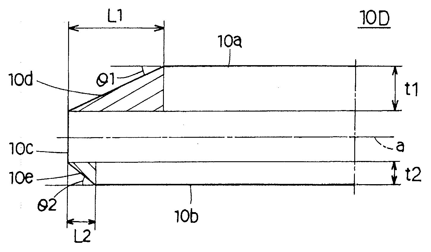
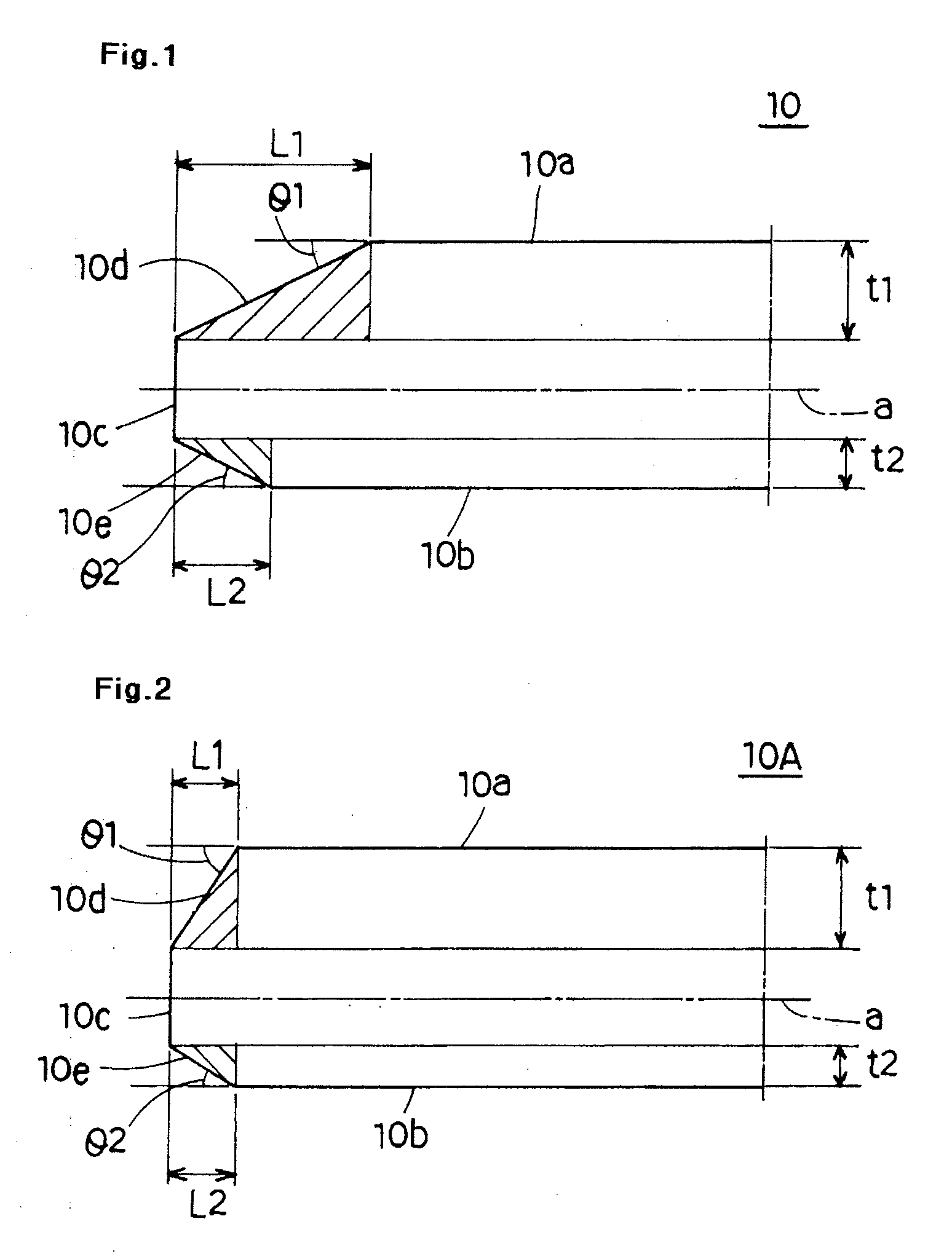
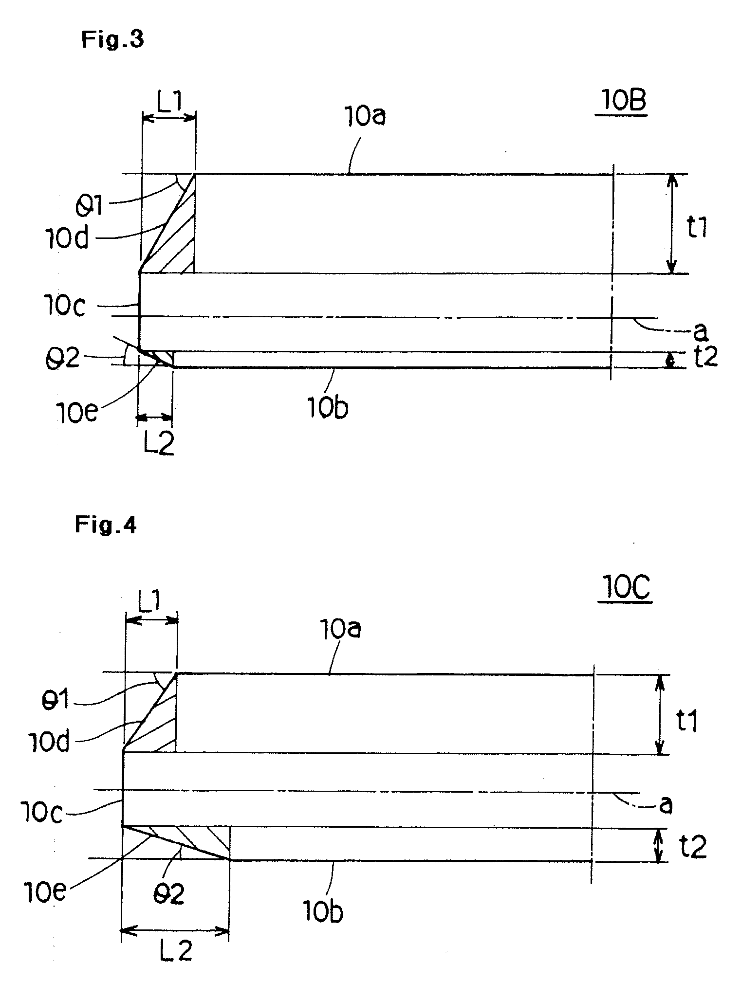
[0031]FIG. 1 shows a silicon wafer 10 (a semiconductor wafer) according to a first embodiment of the present invention. The silicon wafer 10 includes an outer edge surface 10c orthogonally intersecting with a front surface 10a and a back surface 10b and configuring an outermost peripheral edge, a front side-chamfered surface 10d connecting the outer edge surface 10c to the front surface 10a, and a back side-chamfered surface 10e connecting the outer edge surface 10c to the back surface 10b. When viewed in a cleavage plane that orthogonally intersects with the front surface 10a and back surface 10b of the silicon wafer 10, the front side-chamfered surface 10d and the back side-chamfered surface 10e are asymmetric to each other with respect to a virtual line a extending in a diametrical direction of the semiconductor wafer 10 as the center, at half a height of the outer edge surface 10c. In addition, a height t1 of the front side-chamfered surface 10d is greater than a height t2 of th...


PUM

PropertyMeasurementUnit
Lengthaaaaaaaaaa
Angleaaaaaaaaaa
Heightaaaaaaaaaa

Abstract

A semiconductor wafer includes front and back side-chamfered surfaces asymmetric to each other with respect to a virtual line extending in a diametrical direction as the center, at half: the height of the outer edge surface. In addition, the height of the front side-chamfered surface is greater than that of the back side-chamfered surface, causing the front side-chamfered portion to be thicker than the back side-chamfered portion, thereby increasing the number of wafer reclamation cycles.

Description

CROSS-REFERENCE TO RELATED APPLICATIONS[0001]The present application claims priority under 35 U.S.C. §119 of Japanese Application No. 2008-128912, filed on May 15, 2008, the disclosure of which is expressly incorporated by reference herein in its entirety.BACKGROUND OF THE INVENTION[0002]1. Field of the Invention[0003]The present invention relates to semiconductor wafers, more specifically to a semiconductor wafer capable of increasing the number of reclamation cycles.[0004]2. Description of Related Art[0005]In device formation, various inspections are performed in a variety of important processes by using test wafers manufactured from the same ingot that product silicon wafers are manufactured from, the product silicon wafers being shipped from a wafer manufacturing facility. In the device formation, defective wafers are generated in each process, which amount to approximately 30% of the entire wafers processed therein. These test wafers and defective wafers, instead of being disca...

Claims


Application Information

Patent Timeline
IPC IPC(8): B32B3/02
CPCH01L21/02021Y10T428/24777H01L29/0657
Inventor YAMADA, YASUNORI
Owner SUMCO CORP
Why Eureka
Try Eureka