Method of producing fiber, and methods of producing electron-emitting device, electron source, and image display device each using the fiber

Inactive Publication Date: 2005-01-18
CANON KK
View PDF43 Cites 40 Cited by
  • Summary
  • Abstract
  • Description
  • Claims
  • Application Information

AI Technical Summary

Benefits of technology

To successfully use carbon nanotubes in an image display device, it is required to control the integration density of the carbon nanotubes and form a configuration such that an electric field can be uniformly applied to the carbon nanotubes, and moreover, to increase the number of electron emission points (electron emission sites) for increasing the current density per one pixel, while the quantity of electrons emitted from the respective tubes is reduced.
The present invention has been conceived to solve the above-described problems, and it is an object of this invention to provide

Problems solved by technology

However, according to conventional methods of producing carbon nanotubes, it often is difficult to arrange the carbon nanotubes in an array regularly and consistently at appropriate intervals, and to control the density of the carbon nanotubes.
Moreover, since the carbon nanotubes formed b

Method used


Image

  • Method of producing fiber, and methods of producing electron-emitting device, electron source, and image display device each using the fiber
  • Method of producing fiber, and methods of producing electron-emitting device, electron source, and image display device each using the fiber
  • Method of producing fiber, and methods of producing electron-emitting device, electron source, and image display device each using the fiber

Examples


Example

EXAMPLE 1

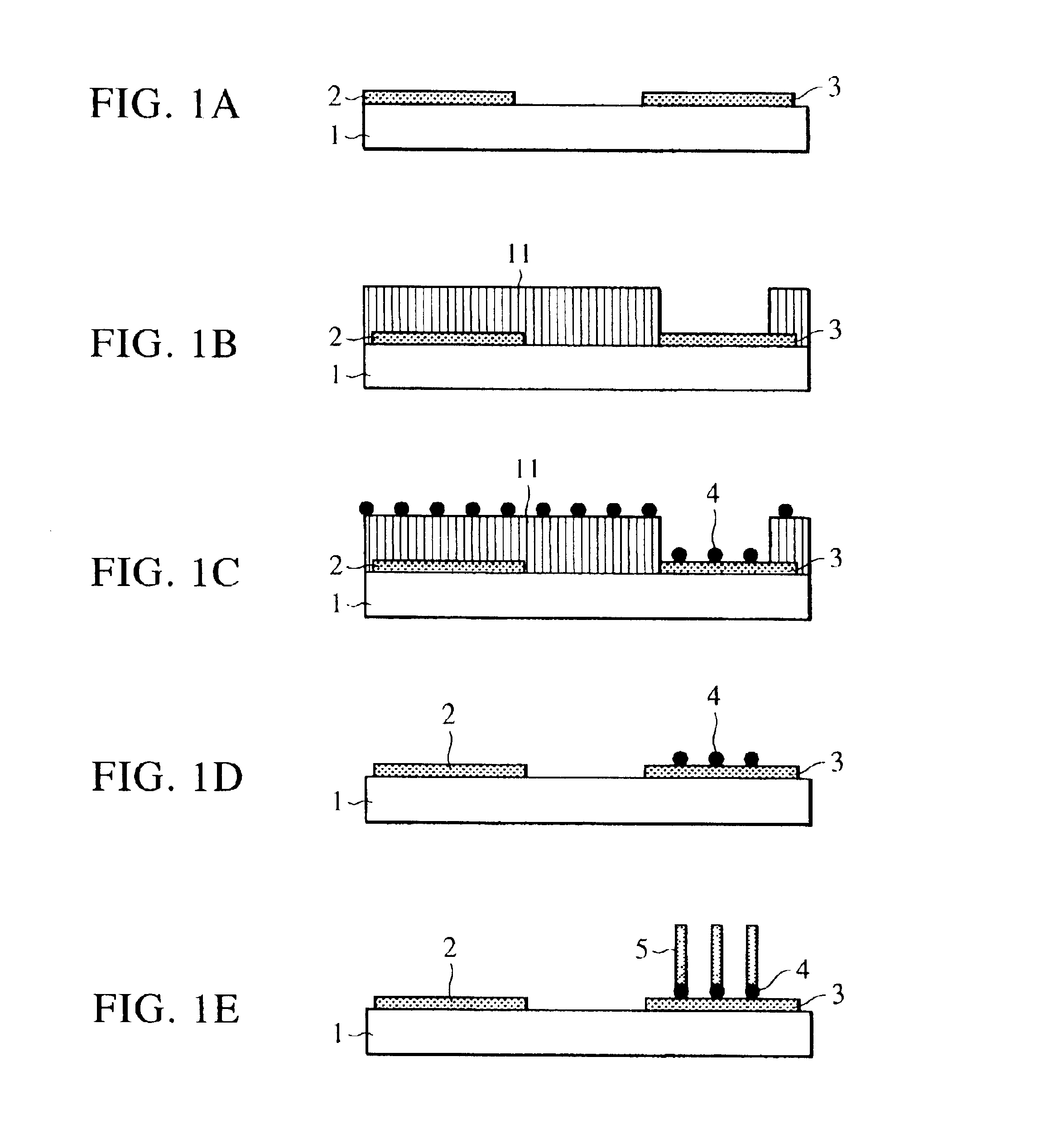
FIGS. 1A to 1E represent steps of a method of producing an electron emitting device in Example 1 of the present invention. FIG. 7 is a plan view showing the prepared electron emitting device. In FIG. 7, reference numeral 5 designates the region in which the fibrous carbon substances are formed. The production process for the electron-emitting device in the Example 1 will now be described below.

(Process 1)

A quartz substrate is used as the substrate 1, and sufficiently rinsed. Ti with a thickness of 5 nm, Pt with a thickness of 50 nm, and Ti with a thickness of 5 nm are vapor-deposited on the substrate in this order as a gate electrode 2 and a cathode 3 by photolithography and sputtering methods (see FIG. 1A).

(Process 2)

Next, a resist pattern 11 is formed using a negative photoresist (see FIG. 1B).

(Process 3)

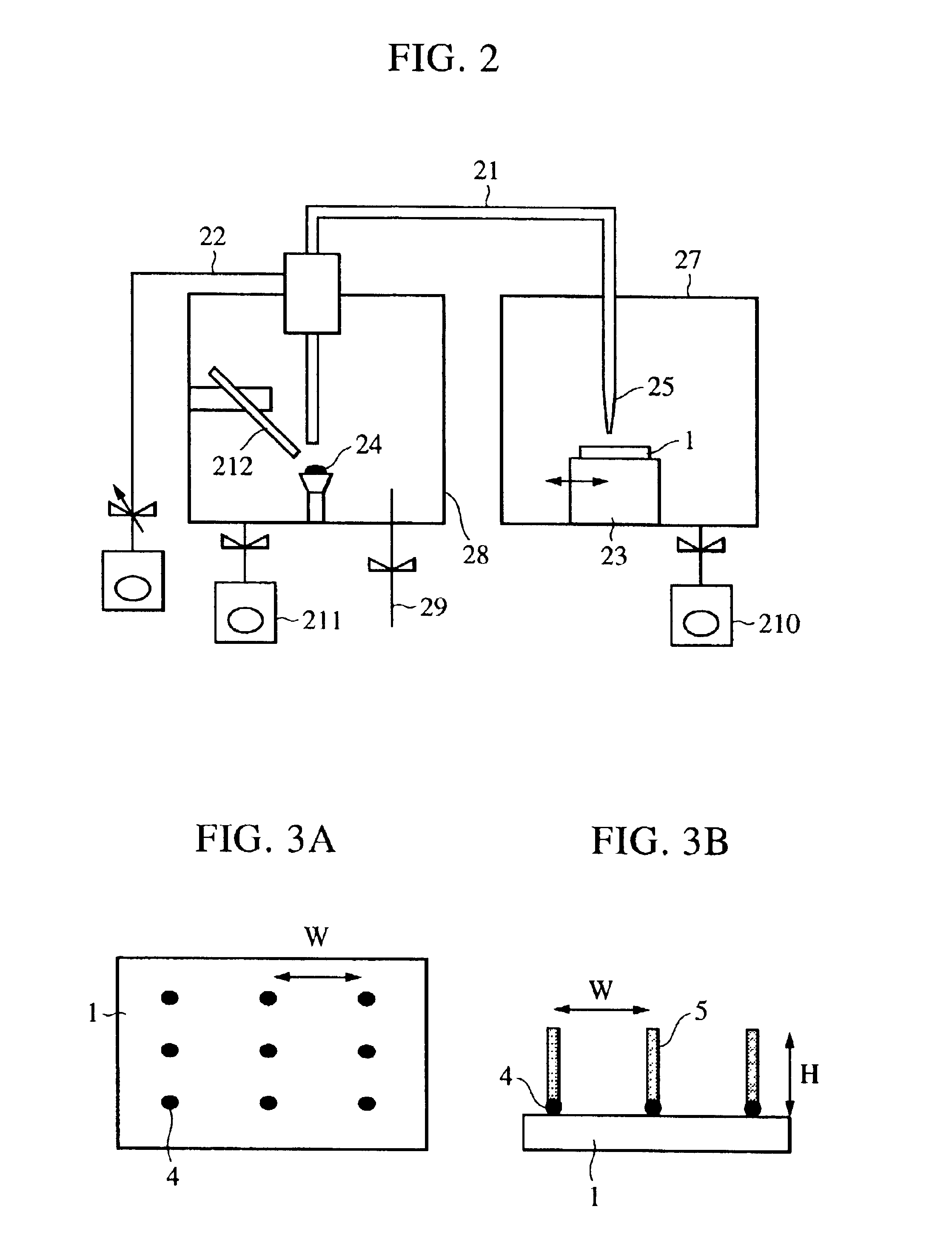
Subsequently, catalytic particles 4 are arranged by a gas deposition method. As shown in FIG. 2, a substrate 1 is disposed on a stage 23 in an arraying chamber 27. Pd as ...

Example

EXAMPLE 2

Hereinafter, Example 2 will be described, in which fibrous carbon substances having different qualities are formed in a manner similar to that in Example 1.

(Process 1)

The gate electrode 2 and the cathode 3 are formed on the quartz substrate 1, and thereafter, the resist pattern 11 is formed in a manner similar to the processes 1 and 2 in Example 1 (see FIG. 1A and FIG. 1B).

(Process 2)

The catalytic particles 4 are arranged in an array by the gas deposition method in a manner similar to the process 3 of Example 1. The conditions under which the particles are formed and arranged in an array are as follows.

Means for evaporating catalyst: resistance heating sublimation method (heating at 1400° C.)

Raw material for catalyst: mixture of Pd and Co

Pressure in forming chamber: 20000 Pa

Pressure in arraying chamber: 100 Pa

Distance d from evaporation portion to transport tube: 10 mm

Shape of employed nozzle: 0.3 mm×5 mm

Movement speed of stage: 10 cm / sec

Distance L between outlet of nozzle ...

Example

EXAMPLE 3

In Example 3, catalytic particles are arranged on a substrate by the gas deposition method, without using a mask, (as an example). FIG. 11 illustrates a method of producing an electron emission device of Example 3.

(Process 1)

Ti with a thickness of 5 nm, Pt with a thickness of 50 nm, and Ti with a thickness of 5 nm are formed on the substrate in this order by the vapor deposition method (see FIG. 11A).

(Process 2)

The catalytic particles 4 are arranged in an array on the substrate 1 by the gas deposition method (FIG. 11B). The conditions for formation and arranging of the particles in an array are as follows.

Means for evaporating catalyst: resistance heating sublimation method (heating at 1400° C.)

Raw material for catalyst: mixture of Pd and Co

Pressure in forming chamber: 50000 Pa

Pressure in arraying chamber: 100 Pa

Distance d from evaporation portion to transport tube: 10 mm

Shape of employed nozzle: 0.5 mm φ

Movement speed of stage: 10 cm / sec

Distance L between outlet of nozzle ...


PUM


Abstract

A method of producing a fiber, comprising the steps of introducing catalytic particles originally formed in a particle-forming chamber into an arraying chamber together with a carrier gas, to cause the catalytic particles to become arranged on a substrate disposed in the arraying chamber. A next step includes growing fibers, each including carbon as a major component, based on the catalytic particles arranged on the substrate. The fibers grow by heating the catalytic particles arranged on the substrate in an atmosphere containing carbon.

Description

BACKGROUND OF THE INVENTION1. Field of the InventionThe present invention relates to a method of producing a fiber containing carbon as a major component, a method of producing an electron-emitting device using the fiber, a method of producing an electron source having a plurality of the electron emitting devices arranged in an array configuration, and a method of producing an image display device comprising the electron source.2. Description of the Related ArtOne type of cold cathode device which has been given attention is the field-emission type (FE type) of electron emitting device which emits electrons from the surface of a material utilizing the known tunnel effect. As an example of the FE type cold cathode, at least one having a cone or quardrangular pyramid shape such as the FE cold cathode disclosed in the publication entitled “physical properties of thin-film field emission cathodes with molybdenum cones”, J. Appl. Phys., 47, 5248 (1976), by Spindt, or the like, has been k...

Claims


Application Information

Patent Timeline
IPC IPC(8): C01B31/00C01B31/02D01F9/127D01F9/12H01J9/02H01J1/304H01J1/30B82B3/00C01B31/04H01J29/04H01J31/12
CPCB82Y10/00B82Y30/00B82Y40/00D01F9/127H01J1/3048H01J9/022C01B31/0233H01J2201/30469C01B32/162C01B32/05H01J1/304H01J9/02
Inventor KITAMURA, SHINTSUKAMOTO, TAKEOISHIKURA, JUNRI
Owner CANON KK
Why Eureka
Try Eureka