

Thermal emission structure
a technology of emission structure and thermal emission, which is applied in the direction of heat storage plant, synthetic resin layered products, inorganic chemistry, etc., can solve the problems of object temperature drop and object temperature ris
- Summary
- Abstract
- Description
- Claims
- Application Information
AI Technical Summary
Benefits of technology
Problems solved by technology
Method used
Image

Examples
embodiment 1
[0077]For Embodiment 1, a description is given with reference to FIGS. 7A and 7B.
[0078]In Embodiment 1, a thermal emission structure 100 is described in which the first conductor layer is composed of a conductive material (non-Phase-change material: metal) which is not a Phase-change material and the second conductor layer is composed of a Phase-change material (vanadium dioxide which is a material that has a higher electrical conductivity in a high-temperature phase than in a low-temperature phase and that has a lower thermal emittance in the high-temperature phase than in the low-temperature phase).
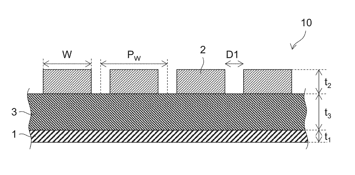
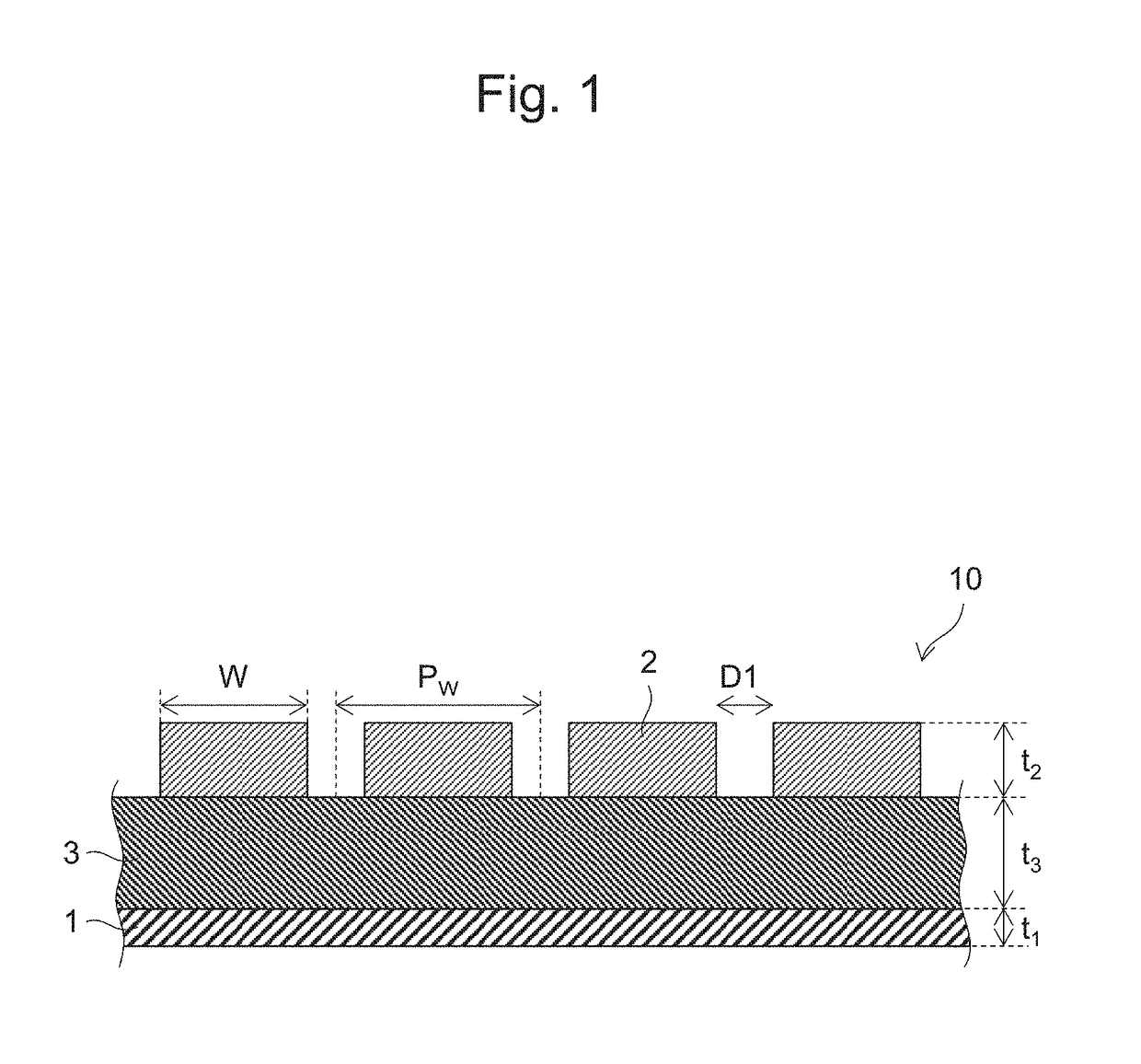
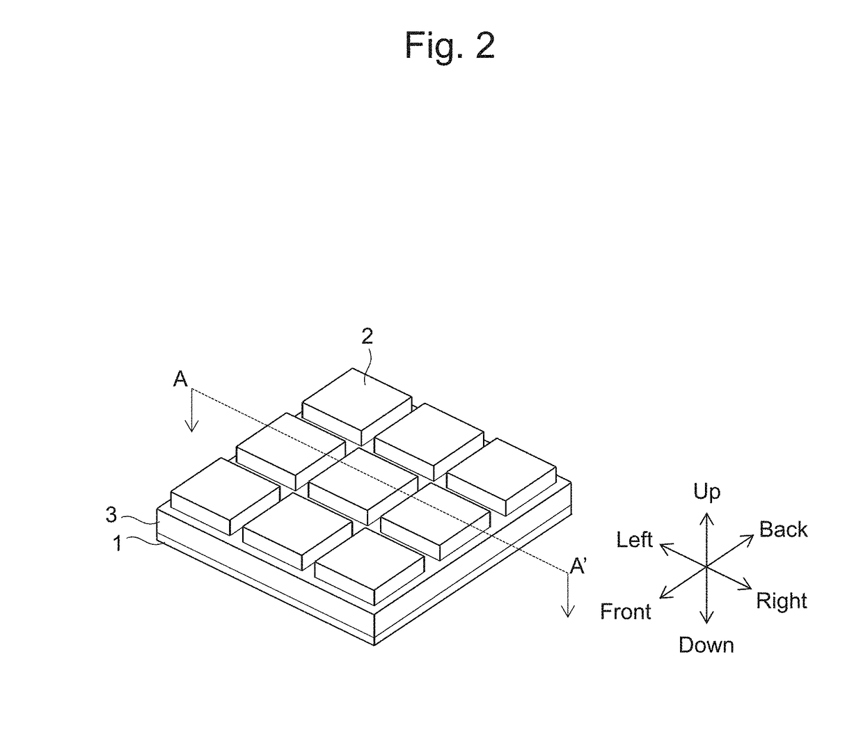
[0079]The first conductor layer 101 is a flat plate-shaped member made of a metal (Al, for example).
[0080]The dielectric layer 103 is a flat plate-shaped member provided on the first conductor layer 101 and composed of a dielectric material (amorphous silicon, for example). The dielectric layer 103 is sandwiched between the first conductor layer 101 and the second conductor layer 102. F...
embodiment 2
[0092]For Embodiment 2, a description is given with reference to FIG. 8.
[0093]Embodiment 2 relates to a thermal emission structure 120 in which the first conductor layer is composed of a Phase-change material (material that has a higher electrical conductivity in a high-temperature phase than in a low-temperature phase and that has a lower thermal emittance in the high-temperature phase than in the low-temperature phase) and the second conductor layer is composed of a non-Phase-change material. Namely, in FIG. 8, the thermal emission structure 120 includes a dielectric layer 123 a first conductor layer 121 that is composed of a Phase-change material (vanadium dioxide, for example) and a second conductor layer 122 that is composed of a non-Phase-change material.
[0094]It should be understood that with the thermal emission structure 120, the same effect as described in Embodiment 1 (namely, the effect of achieving heat release characteristics reverse to those of the used Phase-change m...
embodiment 3
[0095]For Embodiment 3, a description is given with reference to FIG. 9.
[0096]Embodiment 3 relates to a thermal emission structure 130 in which both the first conductor layer and the second conductor layer are composed of a Phase-change material (material that has a higher electrical conductivity in a high-temperature phase than in a low-temperature phase and that has a lower thermal emittance in the high-temperature phase than in the low-temperature phase). Namely, in FIG. 9, the thermal emission structure 130 includes a dielectric layer 133, and a first conductor layer 131 and the second conductor layer 132 both of which are composed of a Phase-change material (vanadium dioxide, for example). In addition, fewer types of materials are used in the thermal emission structure according to this exemplary embodiment, and the thermal emission structure can thus be produced more easily.
[0097]It should be understood that with the thermal emission structure 130, the same effect as described...
PUM
| Property | Measurement | Unit |
|---|---|---|
| Size | aaaaa | aaaaa |
| Size | aaaaa | aaaaa |
| Size | aaaaa | aaaaa |
Abstract
Description
Claims
Application Information