This helps you quickly interpret patents by identifying the three key elements:
Problems solved by technology
Method used
Benefits of technology
Benefits of technology
The present patent provides a solution to improve the efficiency of amplification of transmission signals for a mobile communication terminal using carrier aggregation (CA) communication technology. It proposes a multi-band power amplifier module that can adapt to changes in impedance matching between the output impedance of the power amplifier circuit and the load impedance when the output terminal is connected to a single path or to two paths. The technical effect of the patent is to enhance the efficiency of amplification of transmission signals for a mobile communication terminal usingCA communication technology.
Problems solved by technology
However, U.S. Patent Application Publication No. 2016 / 0119015 does not describe a configuration of the power amplifier module for supporting CA.
Method used
Image
Click on the blue label to locate the original text in one second.
Reading with bidirectional positioning of images and text.
Examples
first embodiment
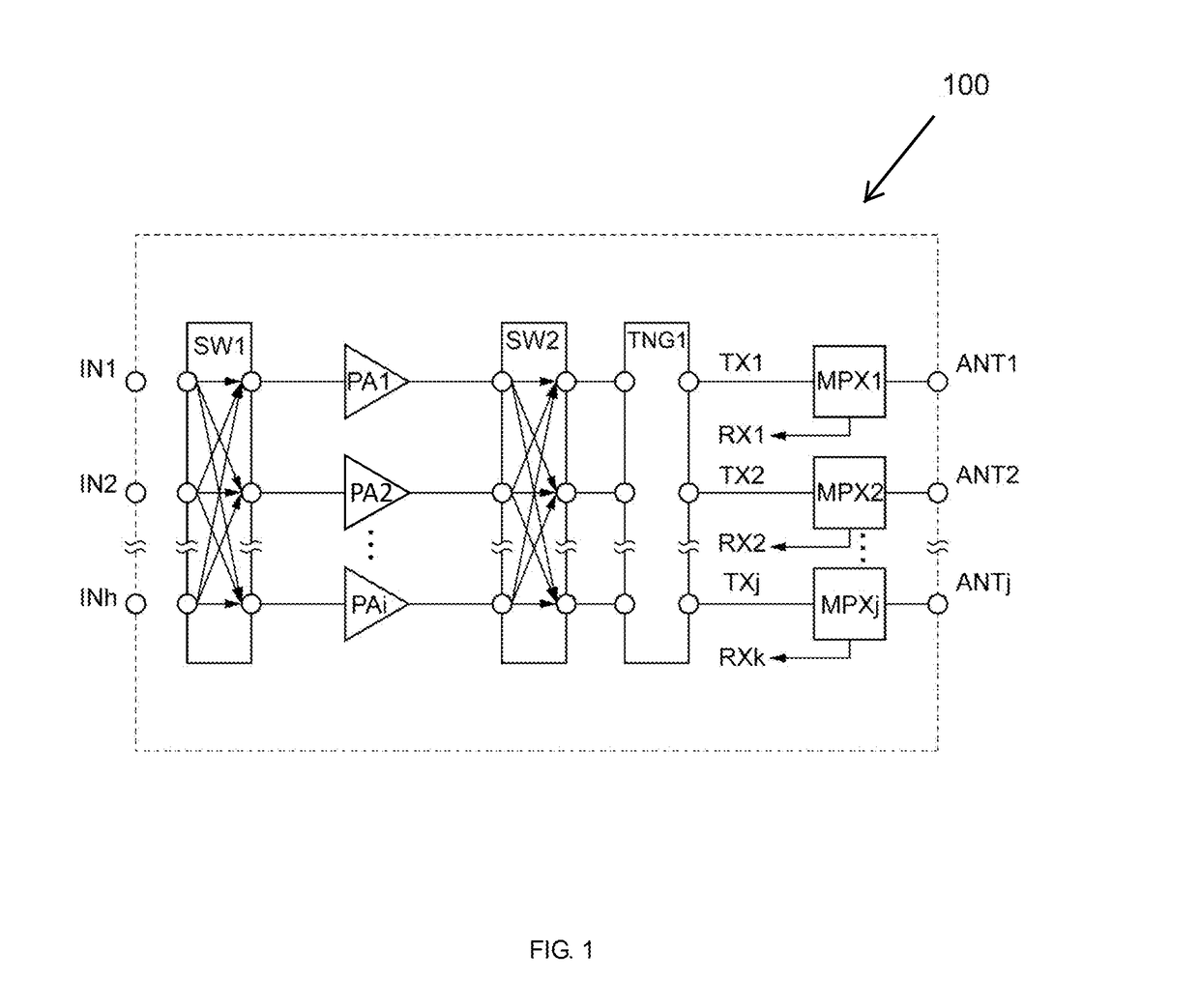
[0019]First, the configuration of a multi-band power amplifier module 100 according to a first embodiment of the present disclosure will be described with reference to FIG. 1. FIG. 1 is a block diagram schematically illustrating a circuit configuration of the multi-band power amplifier module 100 according to the first embodiment.
[0020]The multi-band power amplifier module 100 is a radio-frequency (RF) module included in a mobile communication terminal such as a cellular phone supporting a carrier aggregation (CA) scheme and configured to amplify the power of a transmission signal to a level necessary to transmit the transmission signal to a base station. The transmission signal is, for example, a radio frequency (RF) signal modulated in accordance with a predetermined communication scheme by using a radio frequencyintegrated circuit (RFIC) or the like.
[0021]The CA scheme is a communication scheme for simultaneously sending and receiving a plurality of transmission signals and a pl...
second embodiment
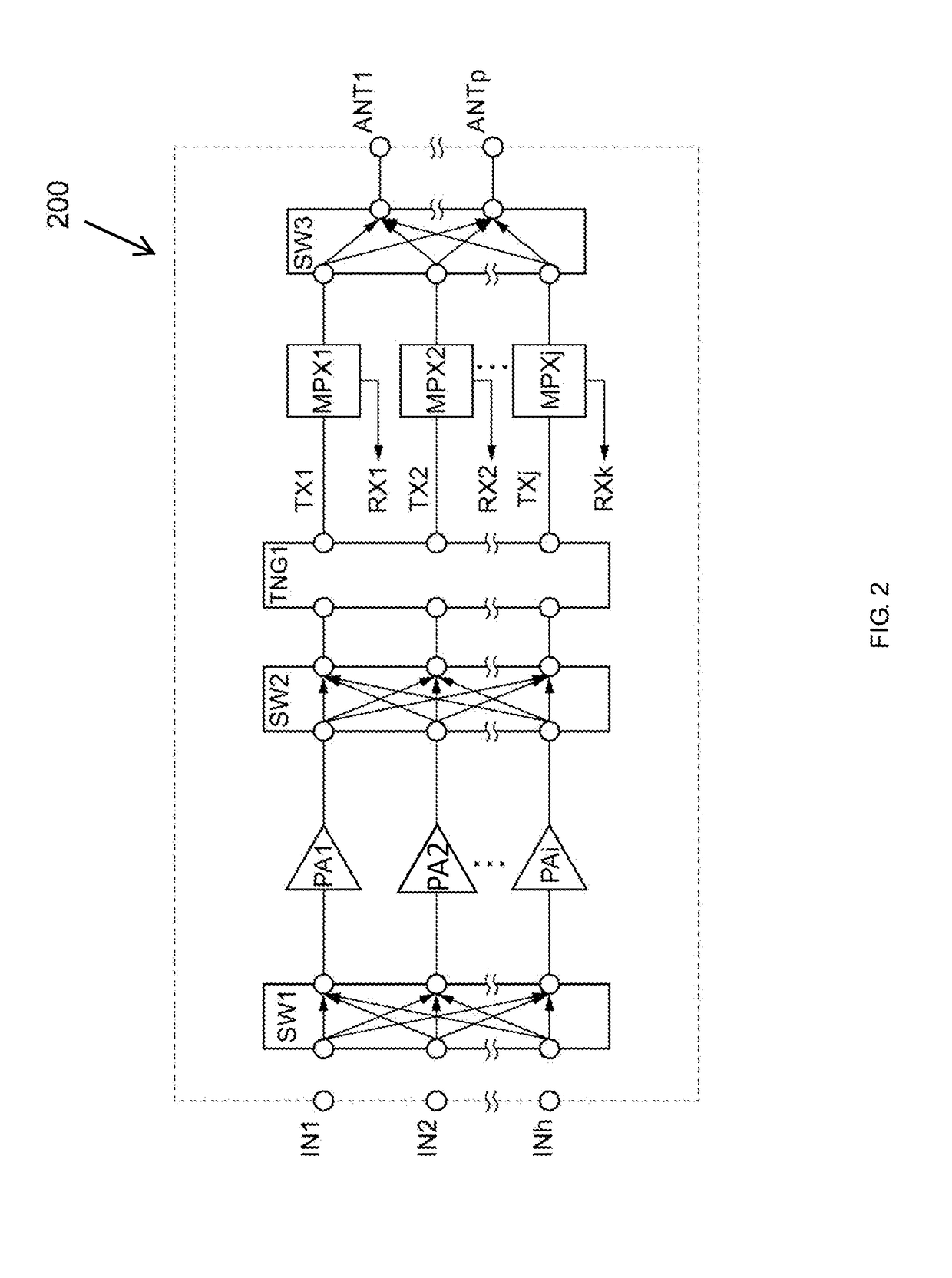
[0041]Next, the configuration of a multi-band power amplifier module 200 according to a second embodiment of the present disclosure will be described with reference to FIG. 2. FIG. 2 is a block diagram schematically illustrating a circuit configuration of the multi-band power amplifier module 200 according to the second embodiment.
[0042]The multi-band power amplifier module 200 includes the plurality of transmission input terminals IN1, IN2, . . . , and INh, the transmission input switch SW1, the plurality of power amplifier circuits PA1, PA2, . . . , and PAi, the transmission output switch SW2, the first tuning circuit TNG1, the plurality of multiplexers MPX1, MPX2, . . . , and MPXj, and a plurality of transmission output terminals ANT1, . . . , and ANTp.
[0043]The multi-band power amplifier module 200 further includes an antenna switch SW3. The antenna switch SW3 switches paths between the plurality of multiplexers MPX1, MPX2, . . . , and MPXj and the plurality of transmission outp...
third embodiment
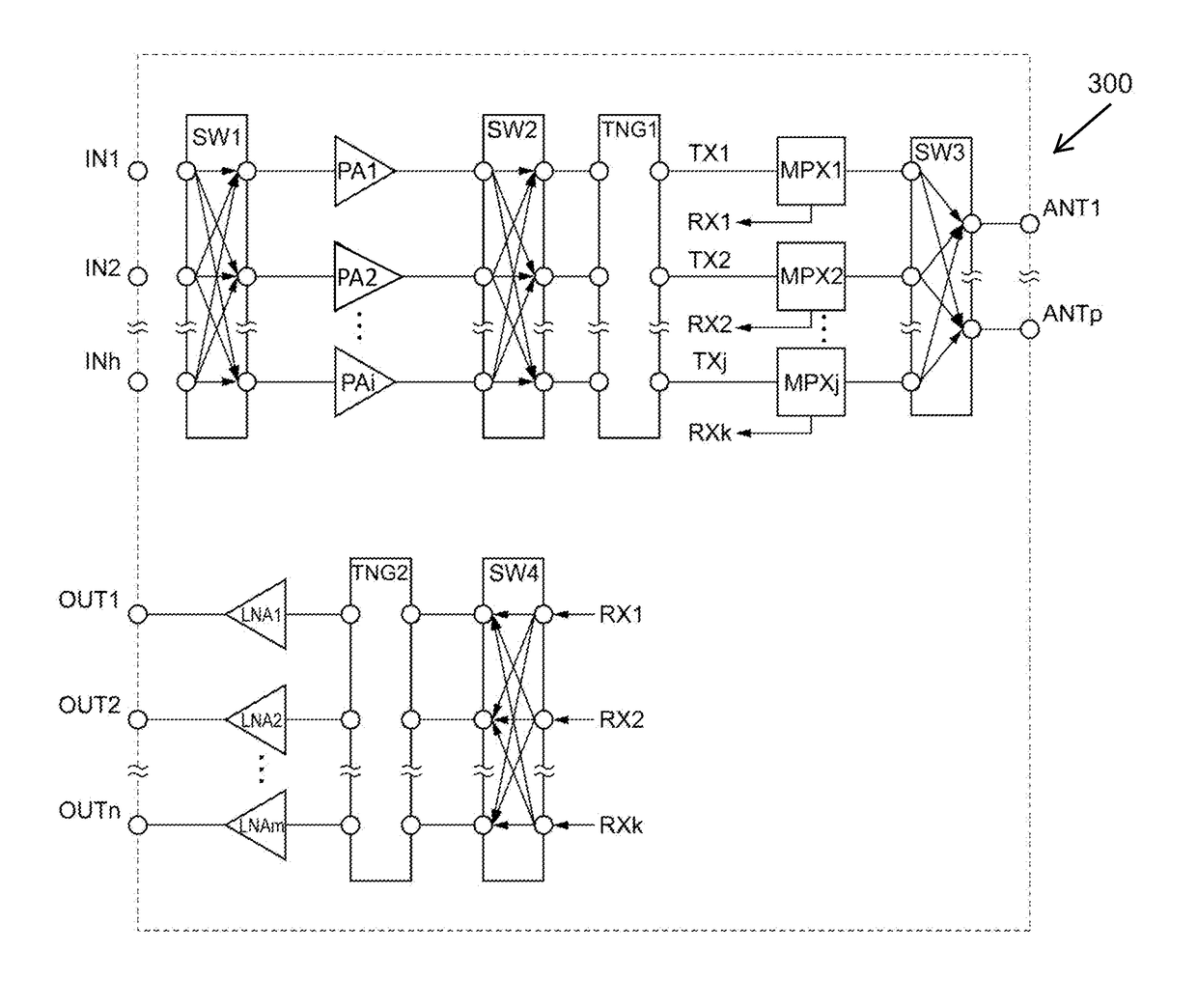
[0045]Next, the configuration of a multi-band power amplifier module 300 according to a third embodiment of the present disclosure will be described with reference to FIG. 3. FIG. 3 is a block diagram schematically illustrating a circuit configuration of the multi-band power amplifier module 300 according to the third embodiment.
[0046]The multi-band power amplifier module 300 includes the plurality of transmission input terminals IN1, IN2, . . . , and INh, the transmission input switch SW1, the plurality of power amplifier circuits PA1, PA2, . . . , and PAi, the transmission output switch SW2, the first tuning circuit TNG1, the plurality of multiplexers MPX1, MPX2, . . . , and MPXj, the antenna switch SW3, and the plurality of transmission output terminals ANT1, . . . , and ANTp.
[0047]The multi-band power amplifier module 300 further includes a reception input switch SW4, a second tuning circuit TNG2, a plurality of low-noise amplifier circuits LNA1, LNA2, . . . , and LNAm, and a pl...
PUM
Abstract
A multi-band power amplifier module includes at least one transmission input terminal, at least one power amplifier circuit that receives a first transmission signal and a second transmission signal through the at least one transmission input terminal, a first filter circuit that allows the first transmission signal to pass therethrough, a second filter circuit that allows the second transmission signal to pass therethrough, at least one transmission output terminal through which the first and second transmission signals output from the first and second filter circuits are output, a transmission output switch that outputs each of the first and second transmission signals output from the at least one power amplifier circuit to the first filter circuit or the second filter circuit, and a first tuning circuit that adjusts impedance matching between the at least one power amplifier circuit and the at least one transmission output terminal.
Description
[0001]This application claims priority from Japanese Patent Application No. 2017-192846 filed on Oct. 2, 2017 and Japanese Patent Application No. 2017-097149 filed on May 16, 2017. The contents of these applications are incorporated herein by reference in its entirety.[0002]The present disclosure relates to a multi-band power amplifier module. Against the backdrop of high-density packaging for mobile communication terminals such as cellular phones, studies are being made on the reduction in the number of components by sharing various components such as an antenna switch, an input switch, an output switch, a duplexer, a power amplifier circuit, a low-noise amplifier circuit, and a matching circuit.[0003]For example, U.S. Patent Application Publication No. 2016 / 0119015 discloses a power amplifier module having M inputs and N outputs, each of at least two or more of the M inputs being coupled to a switch that separates paths. The power amplifier module includes a plurality of filter ci...
Claims
Application Information
Patent Timeline
Application Date:The date an application was filed.
Publication Date:The date a patent or application was officially published.
First Publication Date:The earliest publication date of a patent with the same application number.
Issue Date:Publication date of the patent grant document.
PCT Entry Date:The Entry date of PCT National Phase.
Estimated Expiry Date:The statutory expiry date of a patent right according to the Patent Law, and it is the longest term of protection that the patent right can achieve without the termination of the patent right due to other reasons(Term extension factor has been taken into account ).
Invalid Date:Actual expiry date is based on effective date or publication date of legal transaction data of invalid patent.

