Display device and inspecting method therefor

a display device and display panel technology, applied in the direction of resistance/reactance/impedence, measurement devices, instruments, etc., can solve the problems of signal line disconnections, defect in display panels, crack generation in substrates or stacked layers, etc., to reduce erroneous defect detection, improve inspection accuracy, and accurately determine the progress degree of defects

Active Publication Date: 2018-11-29
SAMSUNG DISPLAY CO LTD
View PDF5 Cites 17 Cited by
  • Summary
  • Abstract
  • Description
  • Claims
  • Application Information

AI Technical Summary

Benefits of technology

[0031]According to exemplary embodiments of the present disclosure, it is possible to improve accuracy regarding the inspection for a defect (e.g., a crack) generated in the display device, to decrease erroneous defect detection, and to accurately determine progress degree of the defect. According to exemplary embodiments, inspection accuracy regarding a defect such as a crack of the display panel may be increased regardless of a wire width deviation by process dispersion in the manufacturing process.

Problems solved by technology

If the display panel receives an impact, a crack may be generated in a substrate or the stacked layers thereon.
The crack may grow larger or spread to other layers or other regions over time, thereby causing a defect in the display panel.
For example, when a crack is generated in the signal lines (e.g., in a data line or a scanning line), the signal lines may become disconnected, a resistance may increase, or moisture may penetrate the display panel through the crack.
In this case, if a fine / micro crack exists in the substrate or the stacked layers of the display panel, even if there is no problem initially, the fine / micro crack may turn into a larger crack due to the warping or the bending of the display panel over time.

Method used


Image

  • Display device and inspecting method therefor
  • Display device and inspecting method therefor
  • Display device and inspecting method therefor

Examples


Embodiment Construction

[0053]Exemplary embodiments of the present disclosure will be described more fully hereinafter with reference to the accompanying drawings. Like reference numerals may refer to like elements throughout the accompanying drawings.

[0054]Spatially relative terms, such as “beneath”, “below”, “lower”, “under”, “above”, “upper”, etc., may be used herein for ease of description to describe one element or feature's relationship to another element(s) or feature(s) as illustrated in the figures. It will be understood that the spatially relative terms are intended to encompass different orientations of the device in use or operation in addition to the orientation depicted in the figures. For example, if the device in the figures is turned over, elements described as “below” or “beneath” or “under” other elements or features would then be oriented “above” the other elements or features. Thus, the exemplary terms “below” and “under” can encompass both an orientation of above and below.

[0055]It wi...


PUM


Abstract

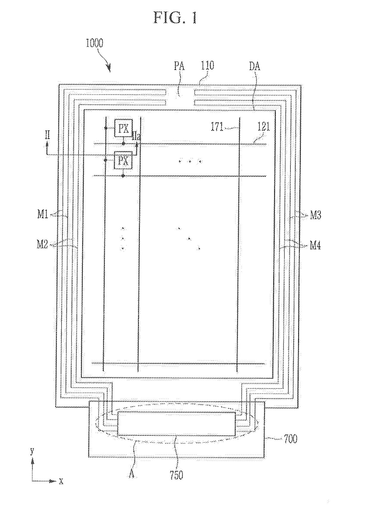
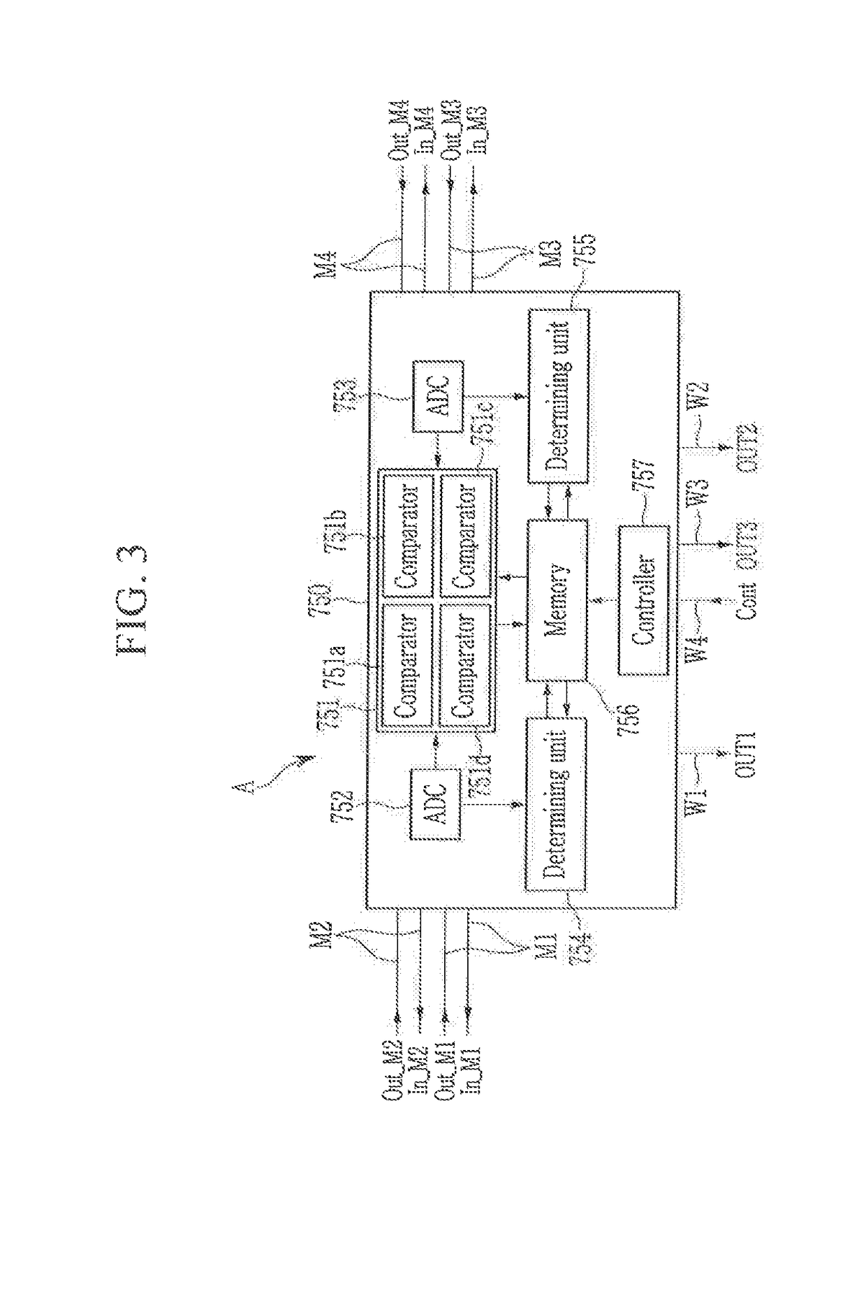
A display device includes a defect inspection circuit, and a display panel having a display area and a peripheral area positioned outside the display area. The display panel includes a sensing wire positioned in the peripheral area and connected to the defect inspection circuit. The defect inspection circuit includes a resistance detection circuit that detects a resistance of the sensing wire based on an output signal corresponding to the sensing wire, a memory that stores first resistance information related to the resistance of the sensing wire detected in a first inspection operation, and a comparator circuit including a first comparator that compares the first resistance information with second resistance information. The second resistance information is related to the resistance of the sensing wire detected in a second inspection operation that is performed at a different time than the first inspection operation.

Description

CROSS-REFERENCE TO RELATED APPLICATIONS[0001]This application claims priority under 35 U.S.C. § 119 to Korean Patent Application No. 10-2017-0063587 filed on May 23, 2017, the entire disclosure of which is incorporated by reference herein in its entirety.TECHNICAL FIELD[0002]Exemplary embodiments of the present disclosure relate to a display device and a method of inspecting a display device for a defect.DISCUSSION OF THE RELATED ART[0003]A display device, such as a liquid crystal display (LCD) or an organic light emitting diode (OLED) display, includes a display panel including a plurality of pixels that display an image, and a plurality of signal lines. Each pixel may include a pixel electrode receiving a data signal. The pixel electrode may be connected to at least one transistor to receive the data signal. The display panel may include a plurality of stacked layers.[0004]If the display panel receives an impact, a crack may be generated in a substrate or the stacked layers thereo...

Claims


Application Information

Patent Timeline
Patent Type & Authority Applications(United States)
IPC IPC(8): G09G3/00G01R27/08
CPCG09G3/006G01R27/08G09G2300/0426G09G2330/12G01R31/2818G01R31/2825G09G3/20
Inventor LEE, KWANG SAESHIM, JUNG HOONKWAK, WON KYUEOM, KI MYEONG
Owner SAMSUNG DISPLAY CO LTD
Why Eureka
Try Eureka