Gate-level mapping of integrated circuits using multi-spectral imaging

Active Publication Date: 2018-12-06
TRUSTEES OF BOSTON UNIV
View PDF0 Cites 1 Cited by
  • Summary
  • Abstract
  • Description
  • Claims
  • Application Information

AI Technical Summary

Benefits of technology

This patent describes a technique for identifying cells in an integrated circuit (IC) by analyzing the way they reflect light at different wavelengths and polarizations. This method reduces the need for high-resolution imaging and is able to detect hardware trojans, which is difficult using traditional electronic testing methods. The technique uses a multi-spectral imaging approach that takes advantage of the modularity of IC design and is non-destructive, measuring the physical layout of the IC. Compared to previous techniques, this method has higher detection rates without the need for controlling for noise or test-vector generation. Overall, this patent provides a faster, more efficient, and non-destructive way to identify and test modifications in IC design.

Problems solved by technology

As such the disclosed techniques cannot be defeated by circuit design techniques such as triggering on rare events or established methods of reducing side channel (e.g. leakage power, delay) signatures.

Method used


Image

  • Gate-level mapping of integrated circuits using multi-spectral imaging
  • Gate-level mapping of integrated circuits using multi-spectral imaging
  • Gate-level mapping of integrated circuits using multi-spectral imaging

Examples


Embodiment Construction

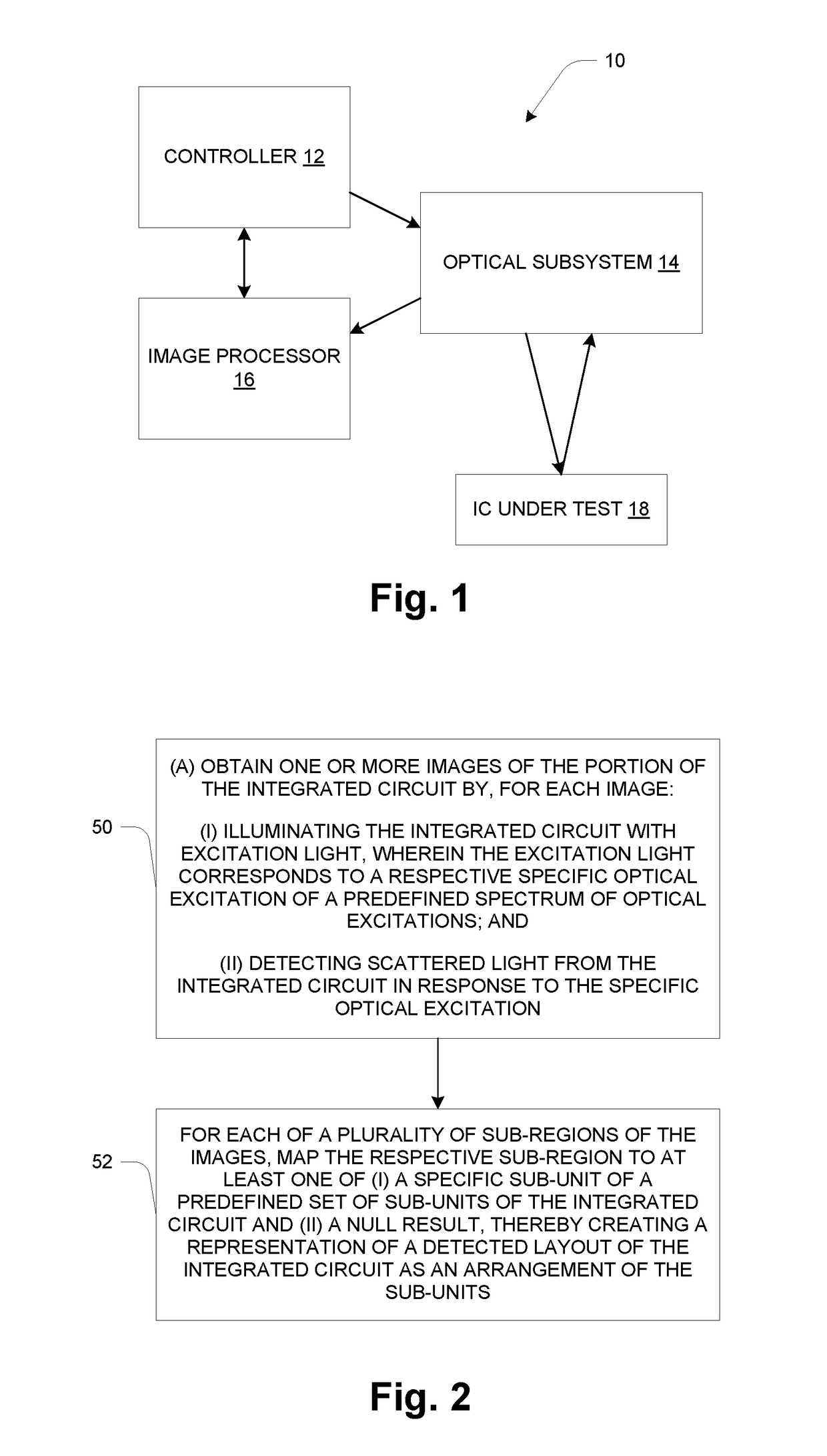
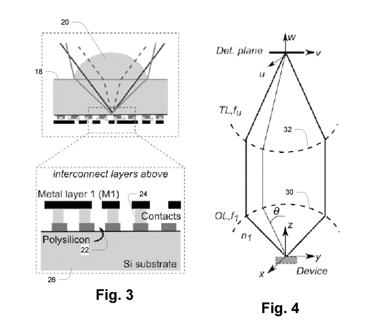
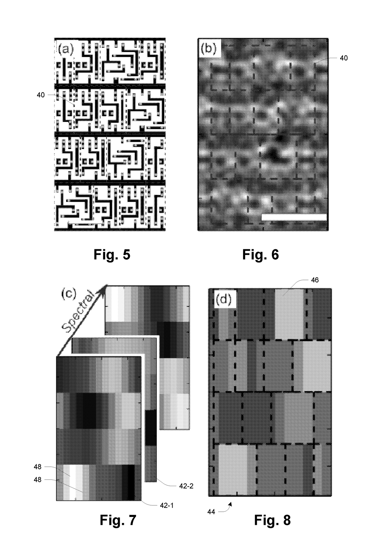
[0039]FIG. 1 shows a testing system 10 including a controller 12, optical subsystem 14, and image processor 16. Under control of the controller 12, the optical subsystem directs optical illumination to an integrated circuit (IC) under test 18 and receives reflected optical energy in response. As described more below, the test system 10 uses a “multi-spectral” approach in which images are obtained from the IC under test 18 for different optical excitations, e.g., illumination at different wavelengths, polarizations, etc. For each optical excitation, the pattern of reflected optical energy is scanned and converted into an electronic representation of a corresponding image of the IC under test 18. These images are processed by the image processor 16, under control of the controller 12, to construct a representation the layout of the IC under test 18.

[0040]FIG. 2 describes aspects of operation, namely optical verification testing of a portion of an IC (e.g., IC under test 18). At 50, th...


PUM


Abstract

Optical verification testing of an IC includes obtaining images of the IC by, for each image: (i) illuminating the IC with excitation light, wherein the excitation light corresponds to a respective specific optical excitation of a predefined spectrum of optical excitations (e.g., wavelength spectrum); and (ii) detecting scattered light from the IC in response to the specific optical excitation. For each of a set of sub-regions of the images, the respective sub-region is mapped to at least one of (i) a specific sub-unit of a predefined set of sub-units (e.g., gates) of the IC and (ii) a null result, thereby creating a representation of a detected layout of the IC as an arrangement of the sub-units. The representation can be used to verify that an as-fabricated layout is consistent with an as-designed layout, to detect unauthorized modifications of the IC structure.

Description

BACKGROUND[0001]The invention is related to the field of integrated circuit verification testing.SUMMARY[0002]Techniques are disclosed for testing whether the layout of an integrated circuit (IC) as manufactured is consistent with the as-designed layout. The advantages of the techniques may be significant due to the high degree of complexity and outsourcing in the modern IC supply chain. Currently the majority of chip designers are ‘fabless’ and outsource the fabrication of their circuits to dedicated foundries. There is a severe emerging threat that circuitry can be modified or added as chip layouts pass through multiple parties during the design and fabrication stages. Such modifications are challenging to prevent and test for and can perform malicious functions such as subverting firewalls, leaking sensitive information or compromising device functionality (e.g. reducing the security of encryption).[0003]Also disclosed are testing techniques based on use of “nanoantenna labels”, ...

Claims


Application Information

Patent Timeline
IPC IPC(8): G06T7/00G06F17/50G01N21/956G01N21/47
CPCG06T7/0006G06F17/5081G01N21/956G01N21/47G06T2207/30148G06T2207/10152G06T2207/20021G06T2207/20081G06T2207/20076G06T7/0002G06T7/0004G06F30/398
Inventor ADATO, RONENJOSHI, AJAYUNLU, M. SELIMGOLDBERG, BENNETT B.
Owner TRUSTEES OF BOSTON UNIV
Why Eureka
Try Eureka