Quality improvement of films deposited on a substrate

a technology of film deposited on a substrate and quality improvement, which is applied in the direction of solid-state diffusion coating, coating, electric discharge tube, etc., can solve the problems of film formation within low thermal budget, such as below 250 degrees celsius, and damage to materials deposited using conventional methods and treated above 250 degrees celsius by elevated temperatures

Inactive Publication Date: 2018-12-06
APPLIED MATERIALS INC
View PDF4 Cites 25 Cited by
  • Summary
  • Abstract
  • Description
  • Claims
  • Application Information

AI Technical Summary

Benefits of technology

[0005]Embodiments of the disclosure generally relate to a method of processing a substrate at a temperature less than 250 degrees Celsius. In one embodiment, the method includes loading the substrate with the deposited film into a pressure vess

Problems solved by technology

Materials deposited using conventional methods and treated above 250 degrees Celsius can be damaged by the elevated temperatures.
However, films formed within low thermals budge

Method used


Image

  • Quality improvement of films deposited on a substrate
  • Quality improvement of films deposited on a substrate
  • Quality improvement of films deposited on a substrate

Examples


Embodiment Construction

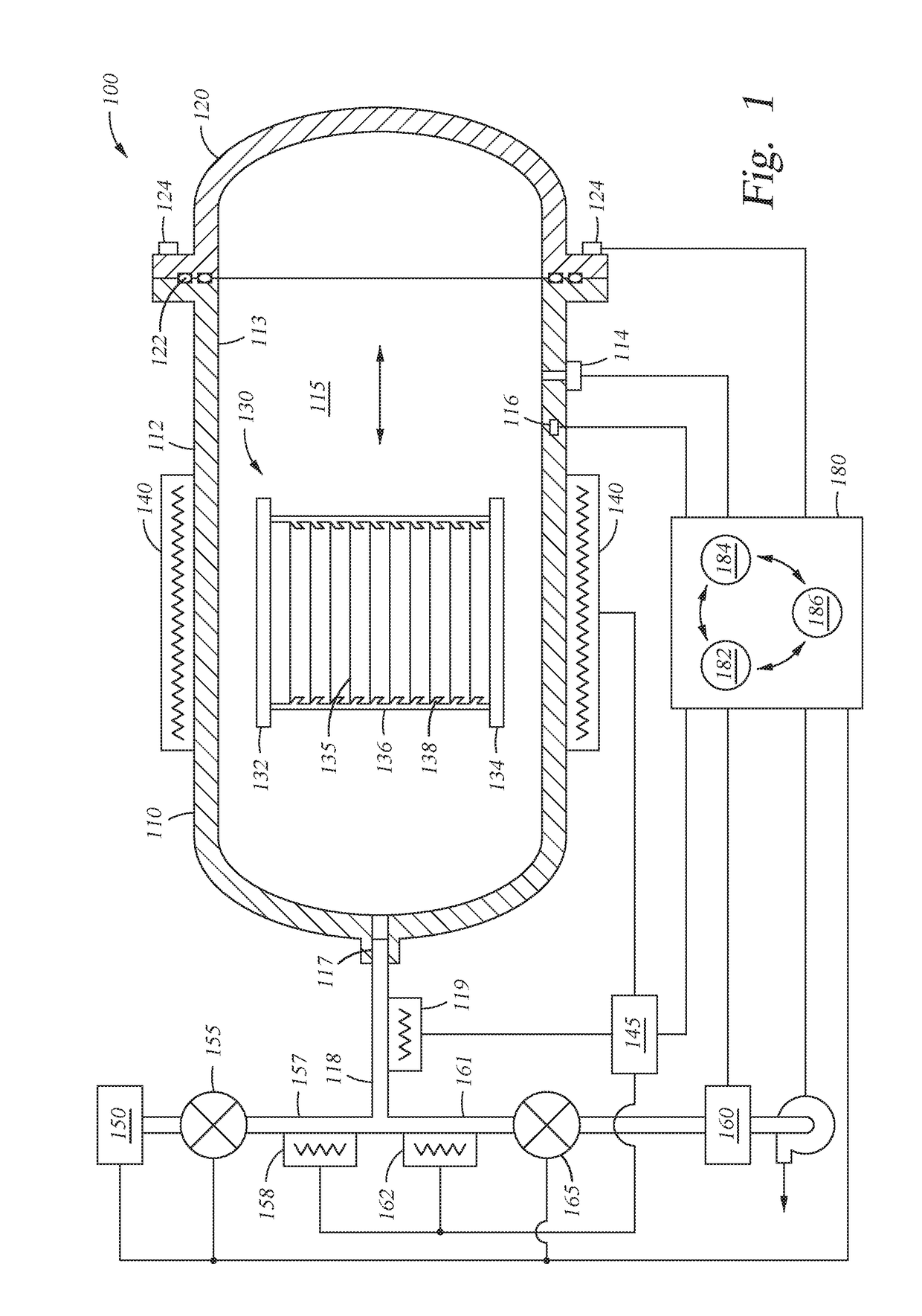
[0014]Embodiments of the disclosure generally relate to a method of improving quality of a film deposited on a semiconductor substrate at a temperature less than 250 degrees Celsius. The method heals regions of a poor-quality film deposited at a temperature less than 200 degrees Celsius. In some embodiments, the film is produced using the Producer® Avila™ plasma enhanced chemical vapor deposition chamber (PECVD) chamber, commercially available from Applied Materials, Inc., of Santa Clara, Calif. In other embodiments, the film may be produced by any chemical vapor deposition (CVD) or physical vapor deposition (PVD) technique, including in chambers produced by other manufacturers. The film is exposed to a processing gas including an oxidizer under high pressure during the post-deposition annealing process disclosed herein, to increase the density of the film. The processing gas penetrates deep into the film layer to reduce the porosity through an oxidation process, thus enhancing the ...


PUM

PropertyMeasurementUnit
Temperatureaaaaaaaaaa
Pressureaaaaaaaaaa

Abstract

Embodiments of the disclosure generally relate to a method of processing a semiconductor substrate at a temperature less than 250 degrees Celsius. In one embodiment, the method includes loading the substrate with the deposited film into a pressure vessel, exposing the substrate to a processing gas comprising an oxidizer at a pressure greater than about 2 bars, and maintaining the pressure vessel at a temperature between a condensation point of the processing gas and about 250 degrees Celsius.

Description

CROSS-REFERENCE TO RELATED APPLICATIONS[0001]This application claims benefit of U.S. provisional patent application Ser. No. 62 / 514,545, filed Jun. 2, 2017, which is herein incorporated by reference.BACKGROUNDField[0002]Embodiments of the disclosure generally relate to fabrication of integrated circuits and particularly to a method of improving quality of a film deposited on a semiconductor substrate.Description of the Related Art[0003]Formation of a semiconductor device, such as memory devices, logic devices, microprocessors, etc., involves deposition of a film over semiconductor substrates. The film is used to create the circuitry for manufacturing the device. Materials deposited using conventional methods and treated above 250 degrees Celsius can be damaged by the elevated temperatures. However, films formed within low thermals budget, such as below 250 degrees Celsius, often have poor quality due to higher porosity and lower density. These films are susceptible to faster etching...

Claims


Application Information

Patent Timeline
IPC IPC(8): H01J37/32
CPCH01J37/32522H01J37/32816H01J37/32715C23C8/12C23C8/16H01J37/32H01L21/02323H01L21/02326H01L21/02337H01L21/0262H01L21/324H01L21/02123H01L21/02532
Inventor MANNA, PRAMITMALLICK, ABHIJIT BASULESCHKIES, KURTISVERHAVERBEKE, STEVENKAMATH, SANJAYWANG, ZONGBINZHANG, HANWENJIANG, SHISHI
Owner APPLIED MATERIALS INC
Why Eureka
Try Eureka