Device and method for measuring height in the presence of thin layers

Inactive Publication Date: 2018-12-20
UNITY SEMICON
View PDF4 Cites 9 Cited by
  • Summary
  • Abstract
  • Description
  • Claims
  • Application Information

AI Technical Summary

Benefits of technology

[0062]The advantage of such an interferometer is that it can be easily integrated, as the core of the interferometer can be remote from the measurement object and only the collimator must be placed in proximity to this object.
[0063]It has the advantage of allowing wide measurement ranges, depending on the delay line selected (of several millimetres or even several centimetres).
[0064]It also has the advantage of allowing measurements of “true” distances, from the point of generation of the reference beam in the collimator to the interfaces of the ob

Problems solved by technology

This configuration is problematic as none of the techniques mentioned above allows satisfactory measurement of the total thickness:The techniques of low-coherence interferometry with detection in the time domain (and an infrared source) allow the thickness of silicon to be measured, but they do not allow the interfaces of the thin layer of polyimide to be distinguished, which are too close com

Method used


Image

  • Device and method for measuring height in the presence of thin layers
  • Device and method for measuring height in the presence of thin layers
  • Device and method for measuring height in the presence of thin layers

Examples


Example

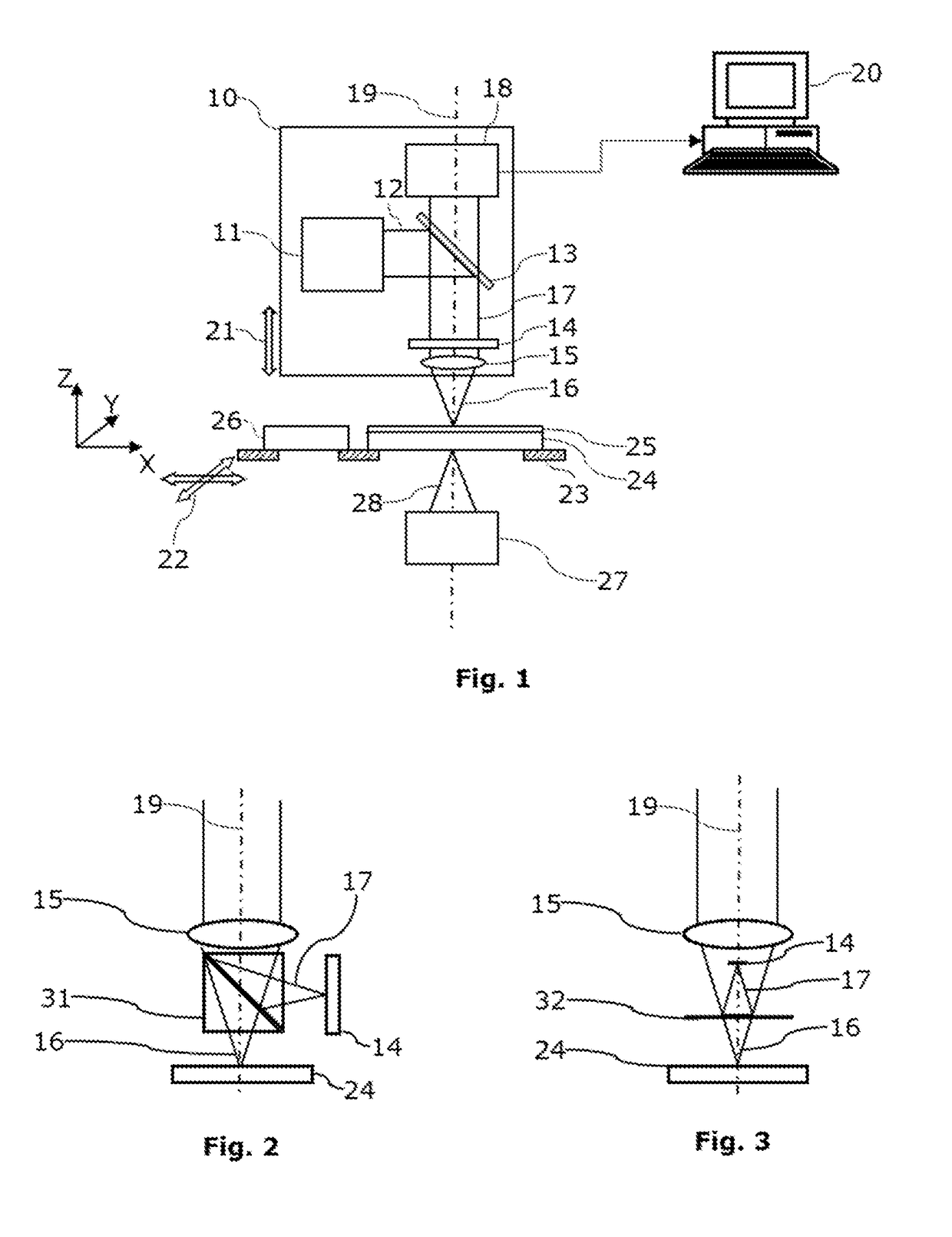
[0097]A first embodiment of the device according to the invention for measuring heights or thicknesses of measurement objects 24 will be described, with reference to FIG. 1.

[0098]In the embodiment presented, the device according to the invention is intended more particularly for measuring measurement objects 24 in the form of wafers 24 while they are being processed.

[0099]As shown, these wafers 24 can comprise one or more thin layers 25 deposited on their surface.

[0100]These wafers 24 can for example comprise a thickness of silicon from 450 μm to 700 μm and a layer of polyimide, silicon oxide, silicon nitride or other transparent dielectrics from some tens of nanometres to some microns.

[0101]Usually these thin layers are at least partially transparent at visible wavelengths. Silicon is transparent at infrared wavelengths. However, depending on the samples, the layer of silicon can comprise opaque layers (component, transistors, metal layers or tracks etc.).

[0102]Under these conditio...


PUM


Abstract

A device for measuring heights and/or thicknesses on a measurement object, includes (i) a first low-coherence interferometer for combining, in one spectrometer, a reference optical beam and a measurement optical beam originating from reflections of the light on interfaces of the measurement object, to produce a grooved spectrum signal with spectral modulation frequencies, (ii) apparatus for measuring an item of position information representative of the relative optical length, (iii) electronic and calculating apparatus arranged for determining at least one spectral modulation frequency representative of an optical path difference between the measurement optical beam and the reference optical beam, and for determining, by exploiting the item of information and the spectral modulation frequency, at least one height and/or thickness on the measurement object, and (iv) second optical apparatus for measuring distance and/or thickness with a second measurement beam incident on the measurement object on a second face opposite the measurement beam.

Description

TECHNICAL FIELD[0001]The present invention relates to a device and a method for measuring heights or thicknesses of samples such as wafers in the presence of thin layers.[0002]The field of the invention is more particularly, but non-limitatively, the field of optical measuring systems for the semiconductor industry.STATE OF THE ART[0003]It is often necessary to perform measurements of height, shape or thickness on wafers during the manufacturing processes of semiconductor components. These measurements can relate for example to surface shapes or flatness, total thicknesses, or thicknesses of layers.[0004]To this end, the use of optical techniques is known, including in particular the techniques of low-coherence interferometry that implement wide-spectrum optical sources. These techniques are essentially of two kinds:[0005]techniques with detection in the time domain;[0006]techniques with detection in the spectral domain.[0007]The techniques with detection in the time domain use a ti...

Claims


Application Information

Patent Timeline
IPC IPC(8): G01B11/06G01B9/02
CPCG01B11/0675G01B9/02021G01B9/02027G01B9/02044G01B9/02057G01B9/02065G01B9/0209G01B2210/44G01B2210/48G01B2290/35
Inventor PIEL, JEAN-PHILIPPESU, JEFF WUYUTHOUY, BENO T
Owner UNITY SEMICON
Why Eureka
Try Eureka