Manufacturing method of a trench power semiconductor device

Active Publication Date: 2019-01-03
SUPER GROUP SEMICON
View PDF1 Cites 3 Cited by
  • Summary
  • Abstract
  • Description
  • Claims
  • Application Information

AI Technical Summary

Benefits of technology

The manufacturing method described in this patent aims to protect the surface of the epitaxial layer and the sidewall of the trench from further oxidization, and to improve the electric field distribution at the bottom of the trench to increase the avalanche voltage of the devices without sacrificing the on-resistance. This is achieved by forming a protective layer on the epitaxial layer and a spacing layer on the sidewall of the trench before forming the interlayer dielectric layer. Additionally, the first sidewall portion of the spacing layer is separate from the bottom of the second sidewall portion to further improve the electric field distribution at the bottom of the trench.

Problems solved by technology

The gate / drain capacitance (Cgd) is an important parameter that can severely affect the switching loss.
If the Cgd is too high, it will result in an increase in the switching loss, which in turn limits the switching speed of the power MOSFETs so that it may be harmful for the power MOSFETs to be used in high frequency circuits.

Method used


Image

  • Manufacturing method of a trench power semiconductor device
  • Manufacturing method of a trench power semiconductor device
  • Manufacturing method of a trench power semiconductor device

Examples


Embodiment Construction

[0012]The aforementioned illustrations and following detailed description are exemplary for the purpose of further explaining the scope of the present disclosure. Other objectives and advantages related to the present disclosure will be illustrated in the following description and appended drawings.

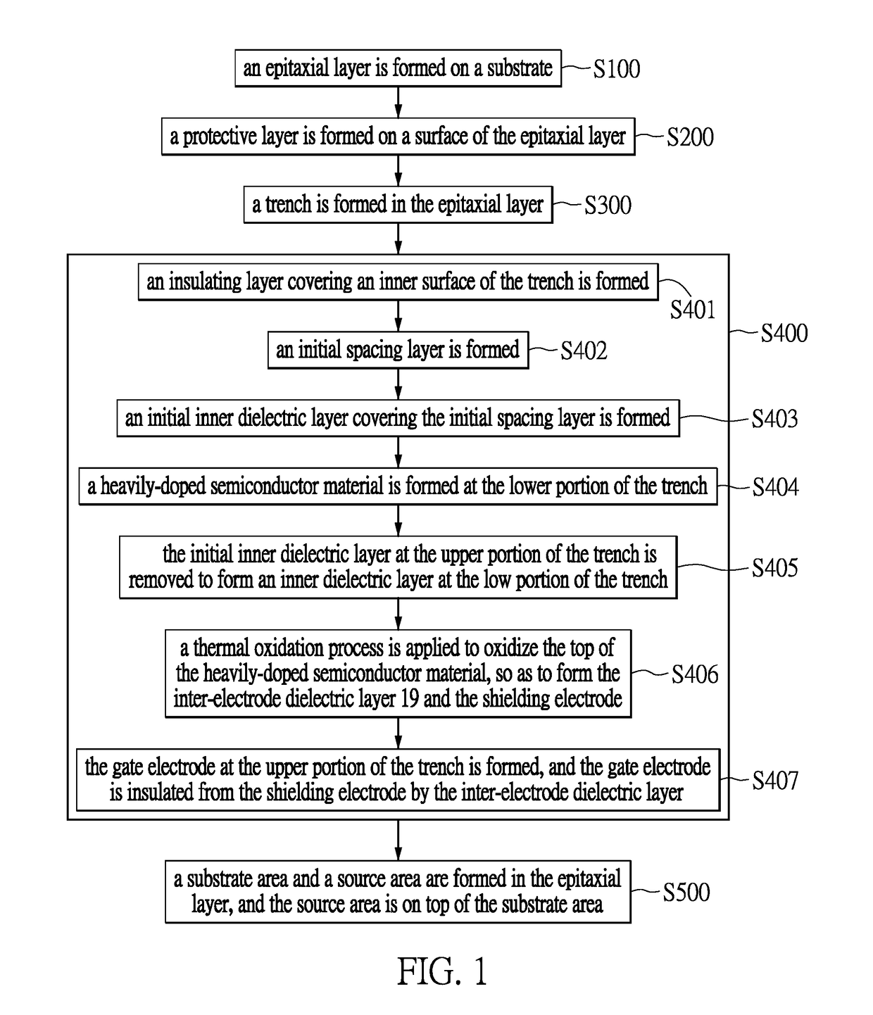
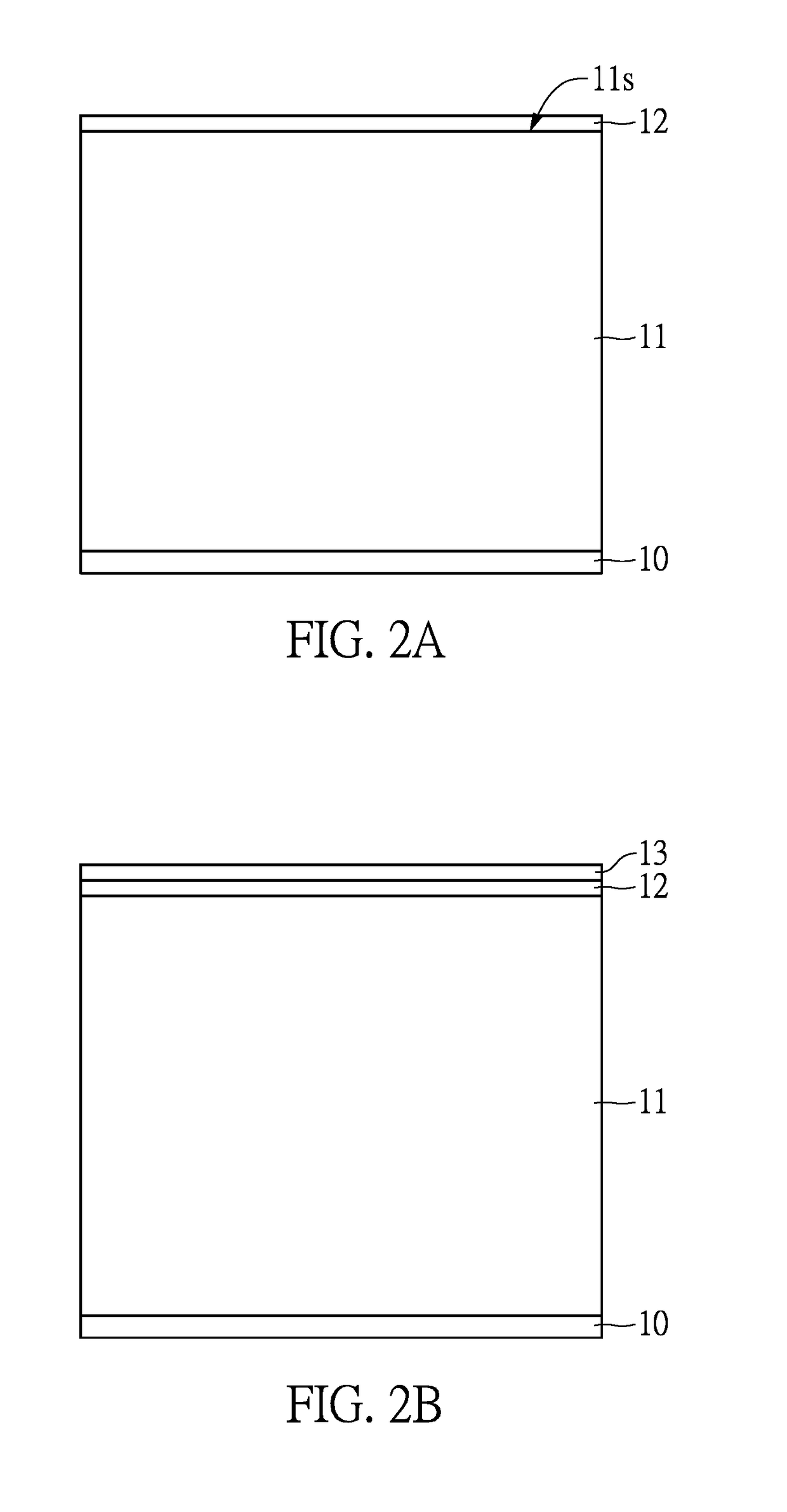
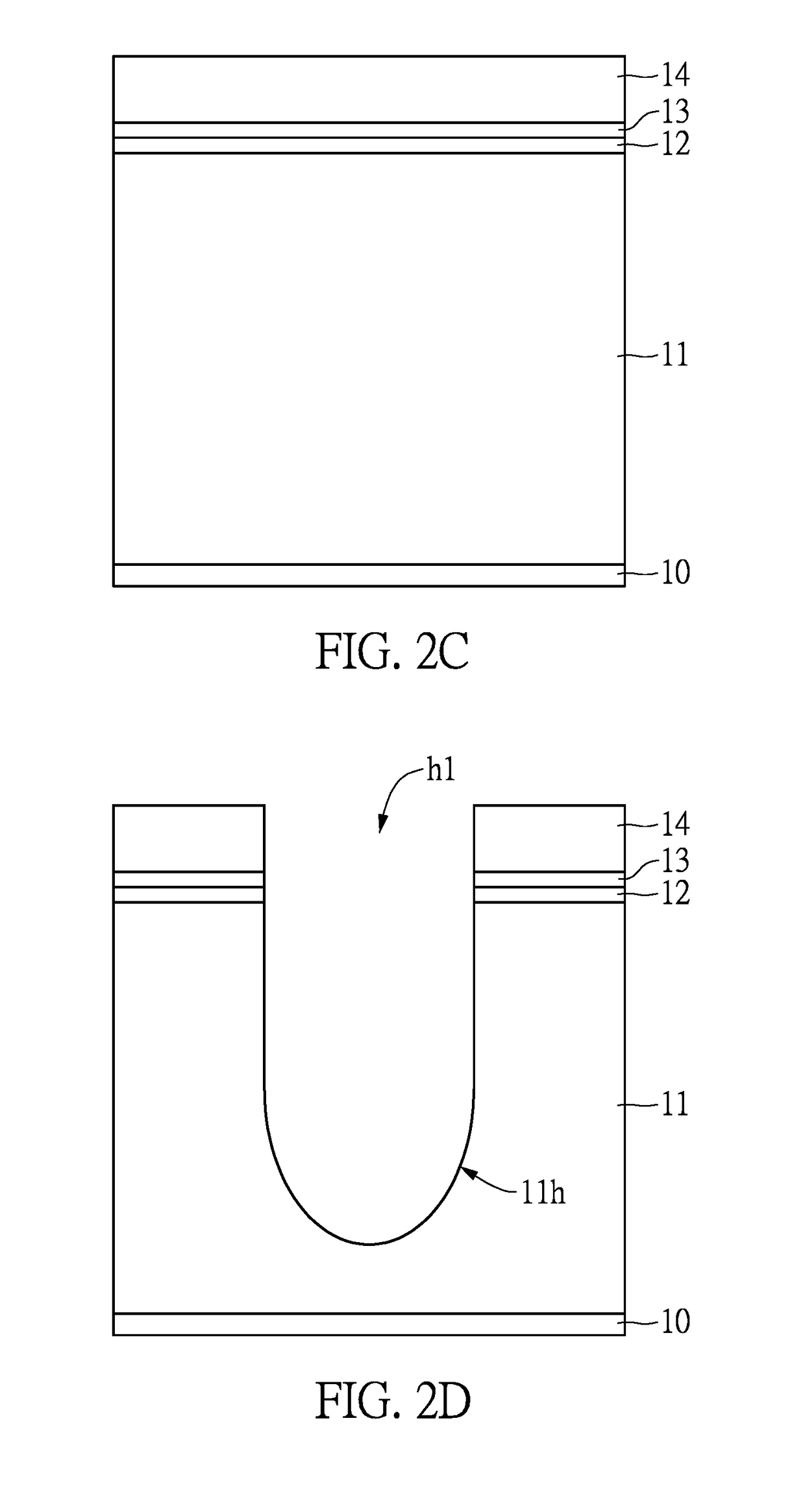
[0013]Reference is made to FIG. 1, where FIG. 1 is a flowchart illustrating a manufacturing method of a trench power semiconductor device according to an embodiment of the present disclosure. Reference is also made to FIGS. 2A-2O, where FIGS. 2A-2O respectively are partial sectional views illustrating trench power semiconductor device at each step of the manufacturing method according to an embodiment of the present disclosure.

[0014]As shown in FIG. 1, in step S100, an epitaxial layer is formed on a substrate and, and in step S200, a protective layer is formed on a surface of the epitaxial layer. FIGS. 2A-2B are referred to collectively in the following description.

[0015]As shown in FIG. ...


PUM


Abstract

A manufacturing method of a trench power semiconductor device is provided. The manufacturing method includes the steps of forming a protective layer on an epitaxial layer and forming a trench gate structure in a trench formed in an epitaxial layer. The trench gate structure includes a shielding electrode, a gate disposed on the shielding electrode and an inter-electrode dielectric layer disposed therebetween. The step of forming the trench gate structure includes forming an insulating layer covering an inner surface of the trench; and before the step of forming the inter-electrode dielectric layer, forming an initial spacing layer, the spacing layer including a first sidewall portion and a second sidewall portion, both of which include bottom end portions spaced apart from each other and extending portions protruding from the protective layer.

Description

BACKGROUND OF THE INVENTION1. Field of the Invention[0001]The present disclosure relates to a manufacturing method of a trench power semiconductor device; more particularly, to a manufacturing method of a trench power semiconductor device with shielding electrodes.2. Description of Related Art[0002]The work losses of current power metal oxide semiconductor field transistors (power MOSFETs) can be classified into two main categories: switching loss and conducting loss. The gate / drain capacitance (Cgd) is an important parameter that can severely affect the switching loss. If the Cgd is too high, it will result in an increase in the switching loss, which in turn limits the switching speed of the power MOSFETs so that it may be harmful for the power MOSFETs to be used in high frequency circuits.[0003]Current power MOSFETs have a shielding electrode located at the lower portion of the gate trench for reducing the Cgd and increasing the avalanche voltage (without sacrificing the on-resist...

Claims


Application Information

Patent Timeline
IPC IPC(8): H01L29/66H01L29/423H01L29/78H01L29/40
CPCH01L29/66734H01L29/4236H01L29/7813H01L29/407H01L29/1095H01L29/41766H01L29/42376H01L29/513
Inventor HSU, HSIU-WENYEH, CHUN-YINGNI, CHUN-WEILEE, YUAN-MING
Owner SUPER GROUP SEMICON
Why Eureka
Try Eureka