Method of forming semiconductor memory device

a technology of memory device and semiconductor, which is applied in the direction of semiconductor devices, digital storage, instruments, etc., can solve the problems of increasing rc delay and achieving poor efficiency, and many defects are formed in the dram cell with the buried gate, so as to improve the effect of rc delay

Active Publication Date: 2019-01-10
UNITED MICROELECTRONICS CORP +1
View PDF15 Cites 3 Cited by
  • Summary
  • Abstract
  • Description
  • Claims
  • Application Information

AI Technical Summary

Benefits of technology

[0006]Overall speaking, the semiconductor memory device of the present invention further performs a two-stepped chemical reaction after forming the storage node pads, to firstly transform the particular spacer followed by removing the transformed spacer via a vaporization process. Through this arrangement, the present invention is able to form the air-gap layer in the spacer structure between the bit lines and the storage node contacts, under a simplified process. That is, the RC delay issue may be improved. Also, since the chemical reaction is specifically performed on the particular spacer within the spacer structure, no other elements may be damage during removing the transformed spacer. That is, the method of the present invention is allowable to form the air-gap layer without causing any damages to any other elements.

Problems solved by technology

However, due to limitations in fabrication technologies, many defects are formed in the DRAM cell with the buried gate.
Furthermore, the shrunk spaces between wires also increase the parasitic capacitance (C), so that, the RC delay is therefore increase to achieve poor efficiency.

Method used


Image

  • Method of forming semiconductor memory device
  • Method of forming semiconductor memory device
  • Method of forming semiconductor memory device

Examples


Embodiment Construction

[0017]To provide a better understanding of the presented invention, preferred embodiments will be described in detail. The preferred embodiments of the present invention are illustrated in the accompanying drawings with numbered elements.

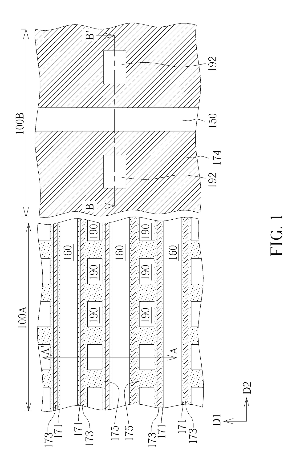
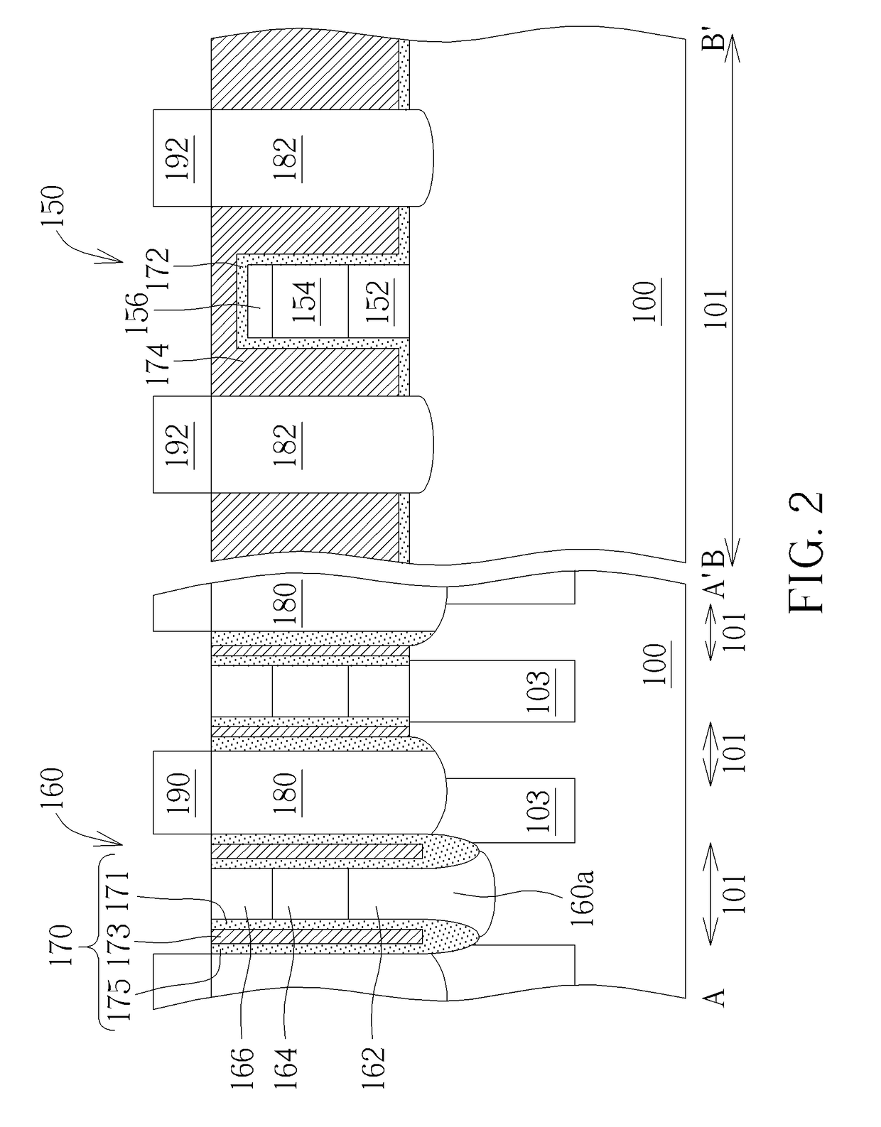
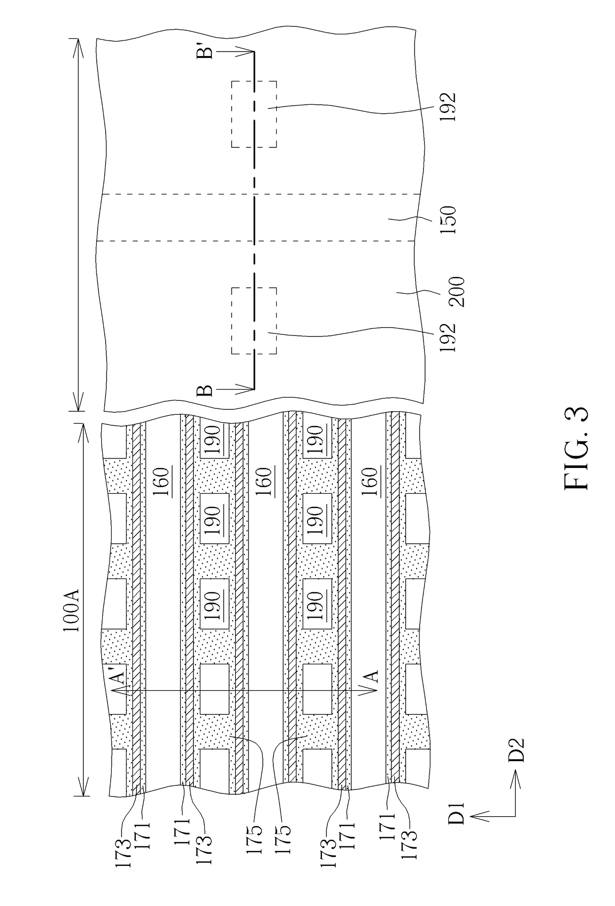
[0018]Please refer to FIG. 1 to FIG. 8, which are schematic diagrams illustrating a forming process of a semiconductor memory device according to the preferred embodiment of the present invention, in which FIG. 1, FIG. 3, FIG. 5 and FIG. 7 show a top view of a semiconductor memory device during different forming steps respectively, and others show a cross-sectional view of a semiconductor memory device during different forming steps respectively.

[0019]The semiconductor memory device of the present embodiment for example includes a dynamic random access memory (DRAM) device, and which includes at least one transistor (not shown in the drawings) and at least one capacitor (not shown in the drawings) , thereto serve as the smallest unit in the DRAM arr...


PUM


Abstract

A method of forming semiconductor memory device includes the following steps. Firstly, a substrate is provided and the substrate includes a cell region. Then, plural bit lines are disposed within the cell region along a first direction, with each of the bit line includes a tri-layered spacer structure disposed at two sides thereof. Next, plural of first plugs are formed within the cell region, with the first plugs being disposed at two sides of each bit lines. Furthermore, plural conductive patterns are formed in alignment with each first plugs. Following theses, a chemical reaction process is performed to modify the material of a middle layer of the tri-layered spacer structure, and a heat treatment process is performed then to remove the modified middle layer, thereto form an air gap layer within the tri-layered spacer structure.

Description

BACKGROUND OF THE INVENTION1. Field of the Invention[0001]The present invention relates to a method of forming a semiconductor memory device, and more particularly, to a method of forming a dynamic random access memory (DRAM) device.2. Description of the Prior Art[0002]For years the trend in the memory industry as well as the semiconductor industry has been to scale down the size of memory cells in order to increase the integration level and thus the memory capacity of DRAM chips. In a DRAM cell with a buried gate, the current leakage caused by a capacitor is often reduced or avoided thanks to a relatively long channel length beneath the buried gate. Therefore, more and more DRAM cells are equipped with buried gates rather than with a conventional planar gate structure due to their superior performances.[0003]In general, the DRAM cells with a buried gate include a transistor device and a charge storage device, which is able to accept signals from a bit line and a word line during th...

Claims


Application Information

Patent Timeline
Patent Type & Authority Applications(United States)
IPC IPC(8): H01L27/108G11C11/401
CPCH01L27/10876G11C11/401H01L27/10823H01L27/14683H10B12/34H10B12/053H10B12/482H10B12/09H01L21/76289H01L29/0649H10B12/485
Inventor CHANG, YI-CHINGCHANG, FENG-YILEE, FU-CHECHEN, CHIEH-TE
Owner UNITED MICROELECTRONICS CORP
Why Eureka
Try Eureka