Unlock instant, AI-driven research and patent intelligence for your innovation.

Addressable vertical nanowire probe arrays and fabrication methods

a nanowire probe and array technology, applied in the field of nanowire probe arrays and fabrication methods, can solve the problems of difficult to maintain the gigaseal between the glass micropipette tip and the cell membrane for more than several hours, and is not scalable to a large number of probes

Active Publication Date: 2019-01-24
RGT UNIV OF CALIFORNIA
View PDF0 Cites 3 Cited by
  • Summary
  • Abstract
  • Description
  • Claims
  • Application Information

AI Technical Summary

Benefits of technology

The invention is a sensor array for detecting neural activity using a special design of vertical nanowires. The nanowires are distributed on a metal pattern on a substrate and are individually electrically addressed. The metal pattern is insulated with dielectric, and the base and stem portions of the nanowires are also preferably insulated. The fabrication process involves patterning metal connections on a substrate and bonding a semiconductor substrate to the metal pattern. The semiconductor substrate is then etched to form the neural nanowire probes that are bonded to the metal pattern. The method allows for the fabrication of a reliable and efficient neural probe sensor array.

Problems solved by technology

Nature 1976, 260 (5554), 799-802] are typically limited single channel measurements and at most less than about ten channels, with tedious and laborious alignment under the microscope, and the gigaseal between glass micropipette tip and the cell membrane is difficult to maintain longer than several hours.
This technology provides the highest fidelity neural recordings of the examples in the previous paragraph, but it is not scalable to large number of probes.
The patch-clamp techniques are also destructive to the cell being probed, and the “one-cell-at-a-time” approach also doesn't resemble the natural configuration of functioning cellular networks.
However, planar microelectrode arrays cannot access the cellular cytoplasm and measure the minute potential changes inside the cell that provides a signature of its physiological state and activity.
To the knowledge of the inventors, no such electrode arrays are fabricated with pitch below 1 μm and / or with individual electrode addressability, leaving the mapping of neural circuits with sub-cellular resolution still impossible, especially at the capacity of intra-cellular probing.
This is a non-controlled process and does not have potential for scaling for multiple electrode sites.
Nature Methods 2010, 7, 200], but this is not scalable to dimensions that permit cell internalization.
None of the prior works using nanowire arrays have resulted in individually addressable nanowires.

Method used


Image

  • Addressable vertical nanowire probe arrays and fabrication methods
  • Addressable vertical nanowire probe arrays and fabrication methods
  • Addressable vertical nanowire probe arrays and fabrication methods

Examples


Embodiment Construction

[0026]A preferred embodiment of the invention is a neural probe sensor array including a substrate with patterned and addressable metal contacts thereon. An array of semiconductor penetrating vertical nanowires are electrically addressed through the addressable metal contacts and extend away from the substrate. The addressable metal contacts are insulated, and stem portions of the nanowires are also preferably insulated.

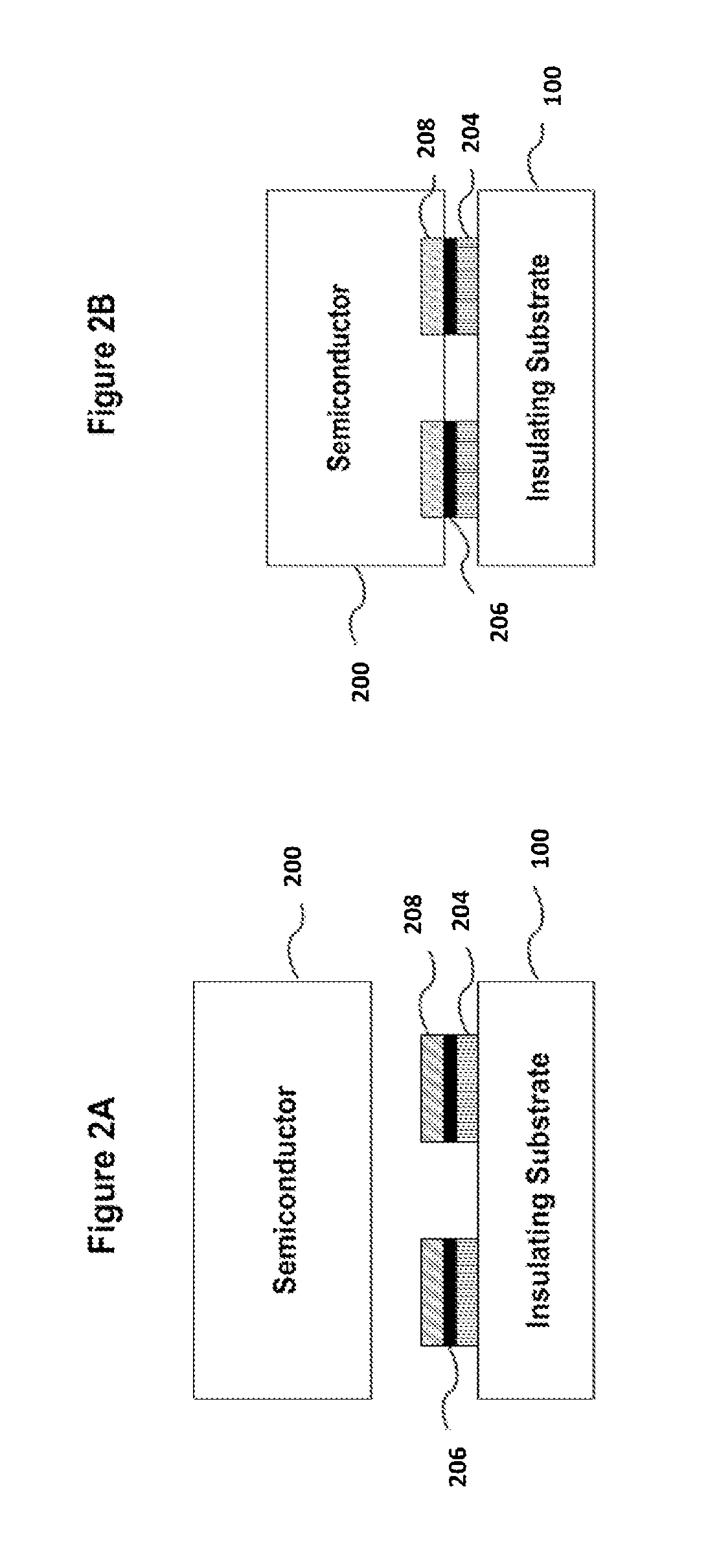
[0027]Preferred methods of fabrication of the invention fabricate a neural probe sensor array by patterning metal connections on a substrate. A semiconductor substrate is bonded to the metal pattern. The semiconductor substrate is etched to form the neural probes that are bonded to the metal pattern. Dielectric is then deposited to insulate the metal pattern, and preferably the stems of the probes are also passivated with the dielectric material.

[0028]Such preferred fabrication methods of the invention are capable of producing high-density arrays of very thin diamete...


PUM

PropertyMeasurementUnit
Fractionaaaaaaaaaa
Distanceaaaaaaaaaa
Distanceaaaaaaaaaa

Abstract

A nanowire probe sensor array including a substrate with a metal pattern thereon. An array of semiconductor vertical nanowire probes extends away from the substrate, and at least some of probes, and preferably all, are individually electrically addressed through the metal pattern. The metal pattern is insulated with dielectric, and base and stem portions of the nanowires are also preferably insulated. A fabrication process patterns metal connections on a substrate. A semiconductor substrate is bonded to the metal pattern. The semiconductor substrate is etched to form the neural nanowire probes that are bonded to the metal pattern. Dielectric is then deposited to insulate the metal pattern.

Description

PRIORITY CLAIM AND REFERENCE TO RELATED APPLICATION[0001]The application claims priority under 35 U.S.C. § 119 and all applicable statutes and treaties from prior U.S. provisional application Ser. No. 62 / 280,366, which was filed Jan. 19, 2016.FIELD[0002]Fields of the invention include nanostructures, biological sensors, neural probes, cardiomyocyte probes, drug screening technologies, drug delivering technologies, and arrays of neural probes.BACKGROUND[0003]Uncovering minute details of the electrophysiological states of excitable cells, such as neurons in the brain or cardiomyocytes in the heart on an individual or network level can advance the understanding of the functional and diseased states of such organs and aid in developing rehabilitation technologies and medicine. The electrophysiological state of the cell is usually studied with sensitive probes that can have access to the interior (cytoplasm) of the cell, thereby enabling the sensitive measurements of the minute potential...

Claims


Application Information

Patent Timeline
IPC IPC(8): A61B5/04B81B1/00B81C1/00G01N33/483
CPCA61B5/04001B81B1/008B81C1/00111G01N33/4836A61B2562/0209A61B2562/0285A61B2562/046A61B2562/125B81B2201/055B81C2201/0132B81C2201/016B81C2203/035B82Y15/00A61B5/24
Inventor DAYEH, SHADI A.CHEN, RENJIELEE, SANG HEONLIU, RENRO, YUN GOOTANAKA, ATSUNORIHWANG, YOONTAE
Owner RGT UNIV OF CALIFORNIA