Method for depositing a group iv semiconductor and related semiconductor device structures

a semiconductor and group iv technology, applied in semiconductor devices, semiconductor/solid-state device details, electrical devices, etc., can solve the problems of reducing the crystal quality of the doped stressor region, affecting the scaling of conventional devices, and affecting the processing efficiency of conventional devices

Active Publication Date: 2019-01-24
ASM IP HLDG BV
View PDF5 Cites 249 Cited by
  • Summary
  • Abstract
  • Description
  • Claims
  • Application Information

AI Technical Summary

Problems solved by technology

However, conventional device scaling faces immense challenges for future technology nodes.
Efforts to increase the p-type carrier density in p-type MOS devices by the addition of further boron may result in a decline in the crystal quality...

Method used


Image

  • Method for depositing a group iv semiconductor and related semiconductor device structures
  • Method for depositing a group iv semiconductor and related semiconductor device structures
  • Method for depositing a group iv semiconductor and related semiconductor device structures

Examples


Embodiment Construction

[0016]Although certain embodiments and examples are disclosed below, it will be understood by those in the art that the invention extends beyond the specifically disclosed embodiments and / or uses of the invention and obvious modifications and equivalents thereof. Thus, it is intended that the scope of the invention disclosed should not be limited by the particular disclosed embodiments described below.

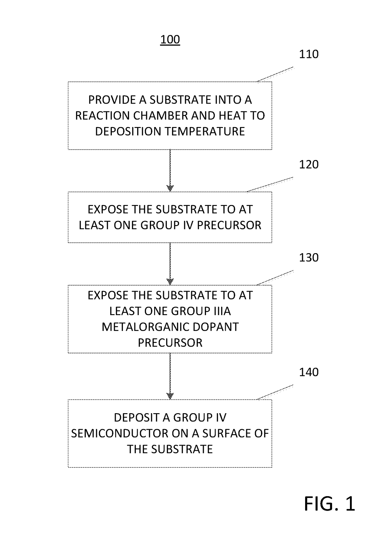
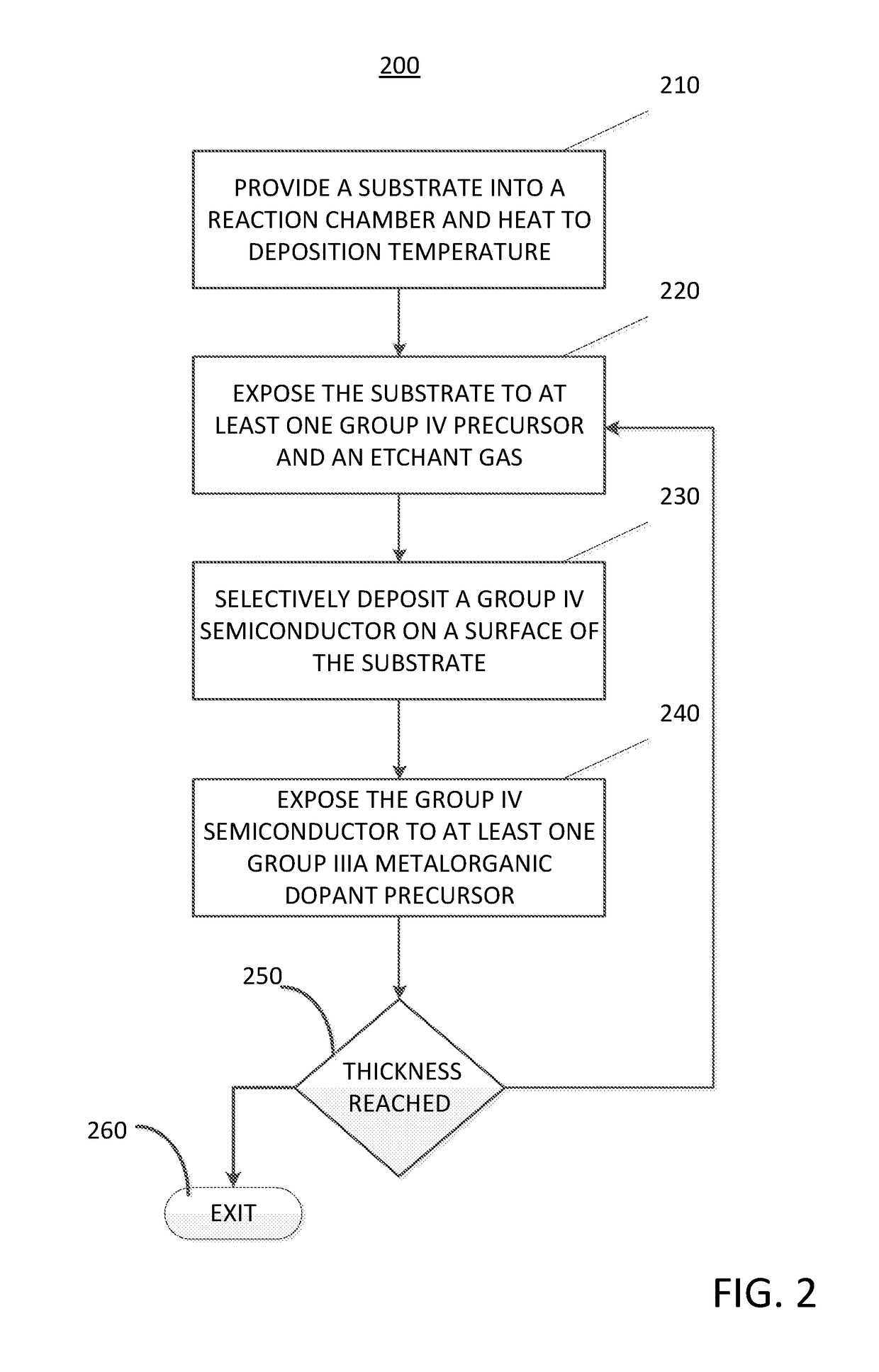
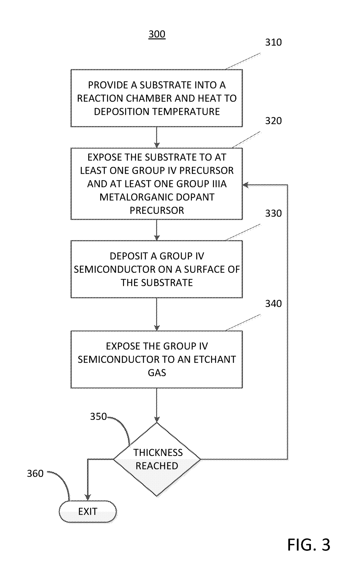
[0017]As used herein, the term “substrate” may refer to any underlying material or materials that may be used, or upon which, a device, a circuit or a film may be formed.

[0018]As used herein, the term “Group IV semiconductor” may refer to a semiconductor material comprising at least one of carbon (C), silicon (Si), germanium (Ge), tin (Sn), or alloys thereof.

[0019]As used herein, the term “Group IIIA metalorganic dopant precursor” may refer to dopant precursor comprising an organic compound containing a metal element, the metal element further comprising a Group IIIA metal.

[0020]As use...


PUM


Abstract

A method for depositing a Group IV semiconductor is disclosed. The method may include, providing a substrate within a reaction chamber and heating the substrate to a deposition temperature. The methods may further include, exposing the substrate to at least one Group IV precursor and exposing the substrate to at least one Group IIIA metalorganic dopant precursor. The methods may further include depositing a Group IV semiconductor on a surface of the substrate. Semiconductor device structures including a Group IV semiconductor deposited by the methods of the disclosure are also provided.

Description

CROSS-REFERENCE TO RELATED PATENT APPLICATION[0001]The present disclosure claims the benefit of U.S. Provisional Patent Application No. 62 / 534,621, filed on Jul. 19, 2017 and entitled “A METHOD FOR DEPOSITING A GROUP IV SEMICONDUCTOR AND RELATED SEMICONDUCTOR DEVICE STRUCTURES,” which is incorporated herein by reference.FIELD OF INVENTION[0002]The present disclosure generally relates to methods for depositing a Group IV semiconductor and related semiconductor device structures. The present disclosure also generally relates to methods of doping a Group IV semiconductor and doping precursors which may be utilized for p-type doping of Group IV semiconductors.BACKGROUND OF THE DISCLOSURE[0003]The scaling of semiconductor device structures, such as, for example, complementary metal-oxide-semiconductor (CMOS) devices, has led to significant improvements in speed and density of integrated circuits. However, conventional device scaling faces immense challenges for future technology nodes.[0...

Claims


Application Information

Patent Timeline
IPC IPC(8): H01L29/66H01L29/78H01L29/165H01L29/167H01L29/08H01L29/45H01L23/535H01L21/02H01L21/285
CPCH01L29/66636H01L29/7851H01L29/7848H01L29/165H01L29/167H01L29/0847H01L29/45H01L23/535H01L29/66795H01L21/02532H01L21/02535H01L21/02529H01L21/02579H01L21/0262H01L21/28518H01L21/28556H01L29/456H01L21/02636H01L29/665H01L29/161
Inventor MARGETIS, JOETOLLE, JOHN
Owner ASM IP HLDG BV
Why Eureka
Try Eureka