Electronic component handler and electronic component tester

a technology of electronic components and handlers, applied in the field of electronic component handlers and electronic component testers, can solve the problems of deteriorating accuracy of determining the presence or absence of an ic device, inability to obtain accurate test results,

Active Publication Date: 2019-01-31
NS TECH INC
View PDF2 Cites 1 Cited by
  • Summary
  • Abstract
  • Description
  • Claims
  • Application Information

AI Technical Summary

Benefits of technology

The patent text describes a configuration that allows for the automatic selection of a specific region on a surface where an electronic component is placed. This eliminates the need for manual selection by an operator and improves the accuracy of determining the presence or absence of the component. The configuration can work regardless of the material used for the surface or the printing material, such as a logo. Overall, this technology simplifies the process of identifying electronic components and improves the accuracy of the determination.

Problems solved by technology

The determination is necessary, because, for example, in a case where the IC device remains in the test socket, the IC device to be tested will overlap the remaining device and there is a concern that an accurate test result cannot be obtained.
When manually setting, for example, in a case where the setting is not appropriate, there is a concern that the accuracy of determining the presence or absence of an IC device deteriorates.

Method used


Image

  • Electronic component handler and electronic component tester
  • Electronic component handler and electronic component tester
  • Electronic component handler and electronic component tester

Examples


first embodiment

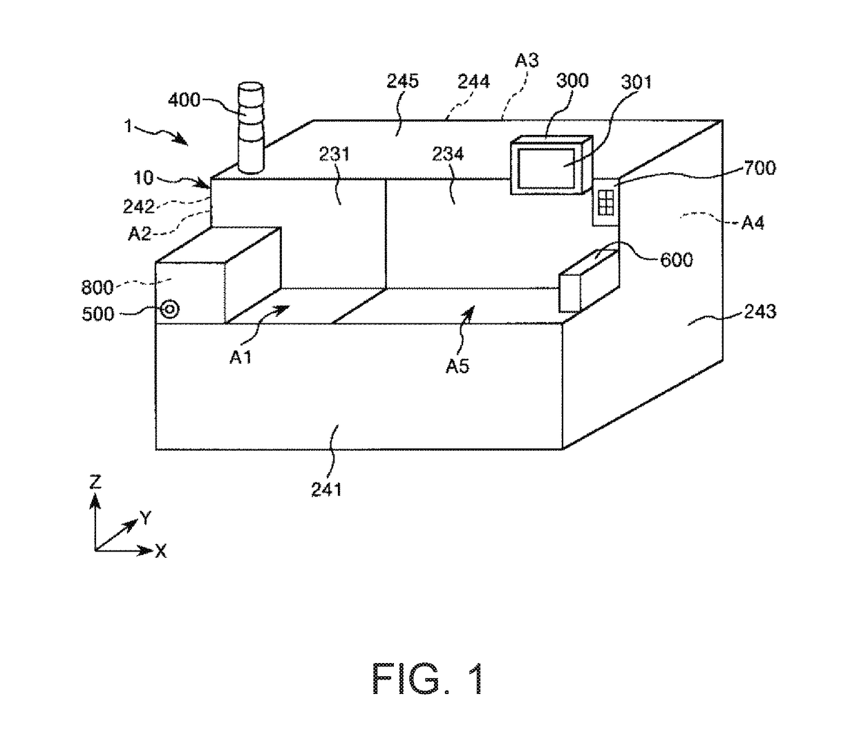
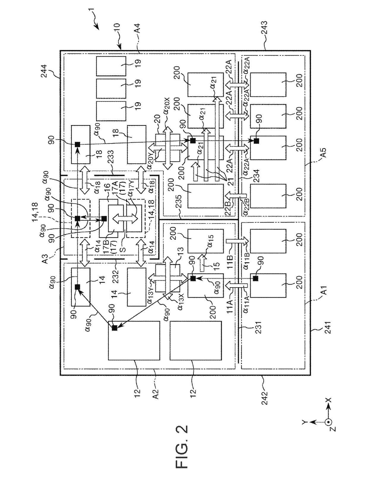
[0055]Hereinafter, a first embodiment of the electronic component handler and the electronic component tester according to the invention will be described with reference to FIGS. 1 to 21. In addition, hereinafter, for the convenience of the description, as illustrated in FIG. 1, three axes which are orthogonal to each other are an X-axis, a Y-axis, and a Z-axis. In addition, an XY plane including the X-axis and the Y-axis is horizontal, and the Z-axis is perpendicular. In addition, a direction parallel to the X-axis is also referred to as “X direction (first direction)”, a direction parallel to the Y-axis is also referred to as “Y direction (second direction)”, and a direction parallel to the Z-axis is also referred to as “Z direction (third direction)”. In addition, a direction in which arrows of each direction are oriented is “positive”, and a direction opposite thereto is “negative”. In addition, “horizontal” referred in the specification is not limited to a complete horizontal s...

second embodiment

[0181]Hereinafter, a second embodiment of the electronic component handler and the electronic component tester according to the invention will be described with reference to FIG. 22, but the description will focus on a point different from the above-described embodiment, and the description of the same contents will be omitted.

[0182]The embodiment is almost similar to the first embodiment except for the control operation of the control unit.

[0183]In the embodiment, when setting the positions of each of the candidate regions A400, the following control operation is performed.

[0184]The control unit 800 sets the plurality of candidate regions A400 having different areas around a predetermined reference point. In other words, in the image D1, squares having different areas with the center S1 of the IC device 90 as a reference point are respectively defined as the candidate region A400. Accordingly, it is possible to set the plurality of candidate regions A400 with a simple control opera...

third embodiment

[0185]Hereinafter, a third embodiment of the electronic component handler and the electronic component tester according to the invention will be described with reference to FIG. 23, but the description will focus on a point different from the above-described embodiments, and the description of the same contents will be omitted.

[0186]The embodiment is almost similar to the first embodiment except for the control operation of the control unit.

[0187]The control unit 800 sets the plurality of candidate regions A400 having different positions of reference points that serve as the center. In other words, while shifting the center of the candidate region A400 from the first candidate region A400, the plurality of candidate regions A400 are set. Accordingly, it is possible to set the plurality of candidate regions A400 with a simple control operation of shifting the candidate region A400 in the arrow direction in FIG. 23 after setting the first candidate region A400.


PUM


Abstract

An electronic component handler includes: a region where an electronic component placement unit on which an electronic component is placed is capable of being disposed; a laser light source which emits light toward the electronic component placement unit placed in the region; a capturing unit which is capable of capturing an image of the electronic component and irradiated with the light; and a processor which determines the presence or absence of the electronic component in the electronic component placement unit based on the image, in which, in the image, the processor sets a first candidate region and a second candidate region from an electronic component placement region which is a region where the electronic component is placed, determines a selected region by comparing the first candidate region and the second candidate region to each other, and performs the determination based on the selected region.

Description

BACKGROUND1. Technical Field[0001]The present invention relates to an electronic component handler and an electronic component tester.2. Related Art[0002]From the related art, there has been known a tester that electrically tests electronic components, such as an IC device (for example, refer to JP-A-2014-196908). In the test apparatus described in JP-A-2014-196908, when performing a test on the IC device, the IC device is transported to a test socket, placed on a test socket, and tested. Further, in the test apparatus described in JP-A-2014-196908, it is determined whether or not the IC device remains in the test socket, that is, the presence or absence of the IC device, prior to performing the test on the IC device. The determination is necessary, because, for example, in a case where the IC device remains in the test socket, the IC device to be tested will overlap the remaining device and there is a concern that an accurate test result cannot be obtained. In addition, in the test...

Claims


Application Information

Patent Timeline
Patent Type & Authority Applications(United States)
IPC IPC(8): G06T7/00G01R31/28
CPCG06T7/0008G01R31/2893G01V8/10G06T2207/30148
Inventor ISHIDA, HIROKAZUKIMURA, YUYATAKAHASHI, TATSUNORI
Owner NS TECH INC
Why Eureka
Try Eureka