High-frequency optoelectronic module

Active Publication Date: 2019-01-31
DUST PHOTONICS LTD
View PDF2 Cites 10 Cited by
  • Summary
  • Abstract
  • Description
  • Claims
  • Application Information

AI Technical Summary

Benefits of technology

[0029]There may be provided a method for operating any of the high-frequency optoelectronic module illustrated in the specification.
[0030]There may be provided a method for exchanging signals with a high-frequency optoelectronic module, the method may include receiving, by at least one optoelectronic circuit of the high-frequency optoelectronic module, high-frequency output electrical signals from a first chip of the high-frequency optoelectronic module; converting, by the at least one optoelectronic circuit, the high-frequency output electrical signals to high-frequency output optical signals; outputting by the by the at least one optoelectronic circuit, the high-frequency output optical signals; receiving, by at least one optoelectronic circuit of the high-frequency optoelectronic module, high-frequency input optical signals sent towards the first chip; converting, by the at least one optoelectronic circuit, the high-frequency input optical signals to high-frequency input electrical signals; and outputting to the first chip, by the by the at least one optoelectronic circuit, the high-frequency input electrical signals. The first chip may include a set of high-frequency electrical input/output (IO) interfaces. The at least one optoelectronic unit comprises a group of high-frequency electrical IO interfaces and a group of high-frequency optical IO interfaces. The group of high-frequency optical IO interfaces is coupled to the group of high-frequency electrical IO interfaces; wherein the high-frequency optoelectronic module comprises a substrate that is coupled to the first chip and the at least one optoelectronic chip; wherein the set of high-frequency electrical IO interfaces is coupled to the group of high-frequency electrical IO interfaces via a group of conductors; wherein a length of each conductor of the group of conductors is of a scale that does not exceed a millimetric scale; wherein the high-frequency it not smaller than one hundred gigabits per second. Any exchange of signals bet

Problems solved by technology

The ever-growing increase in global internet traffic imposes significant challenges on data center operators.
The number of input/output (IO) ports on these large switch application specific integrated circuits (ASICs) is limited by package and printed circuit board (PCB) design rules, with 256 ports being the upper limit, so far.
However, the powe

Method used


Image

  • High-frequency optoelectronic module
  • High-frequency optoelectronic module
  • High-frequency optoelectronic module

Examples


Example

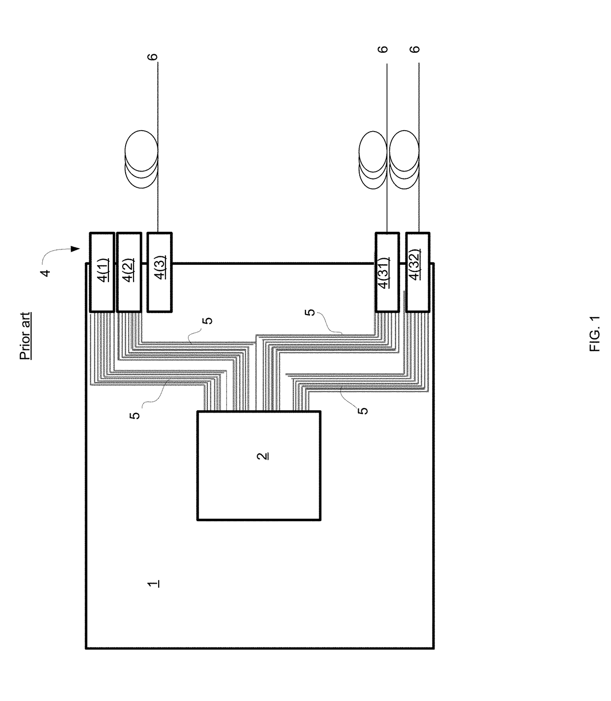
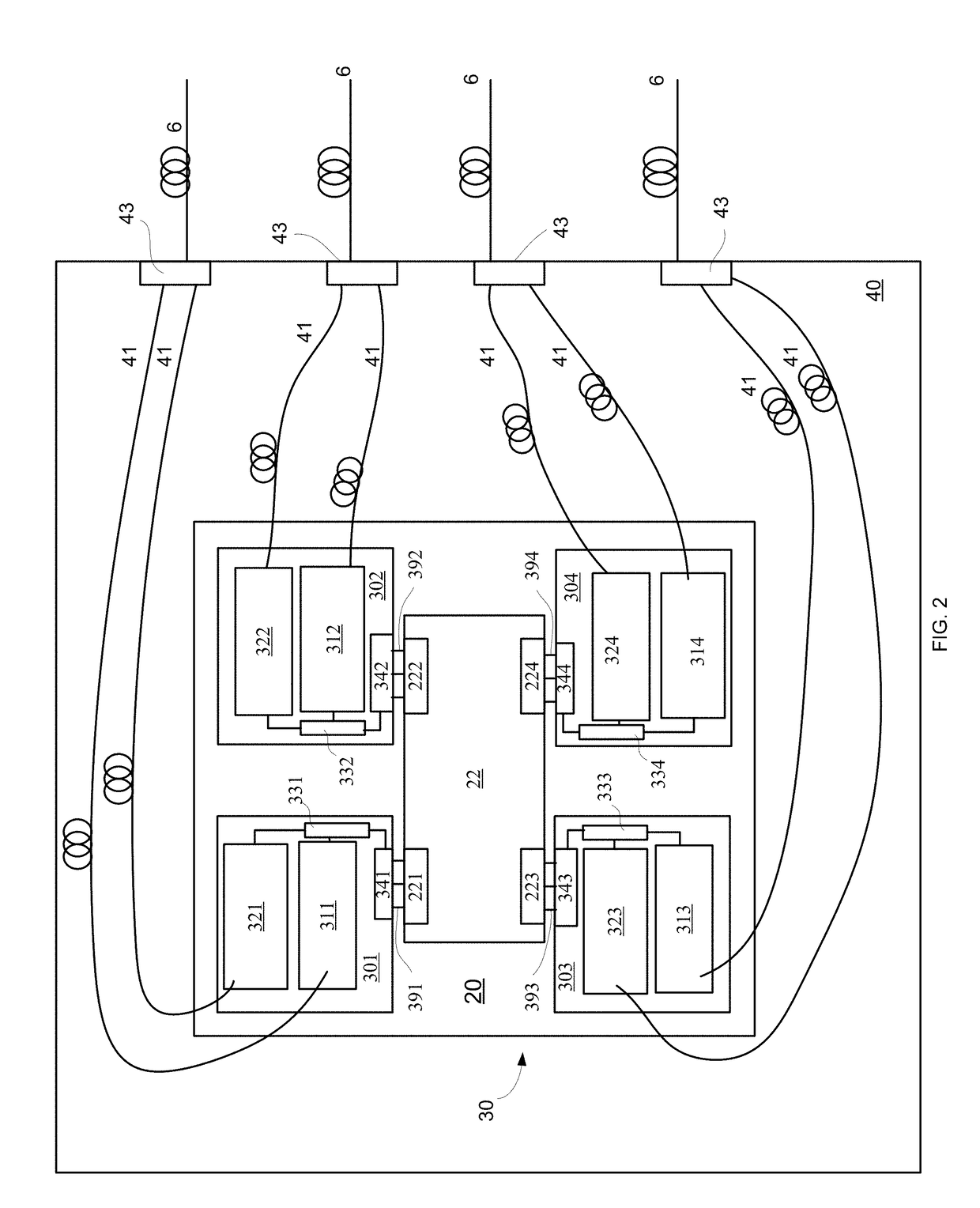
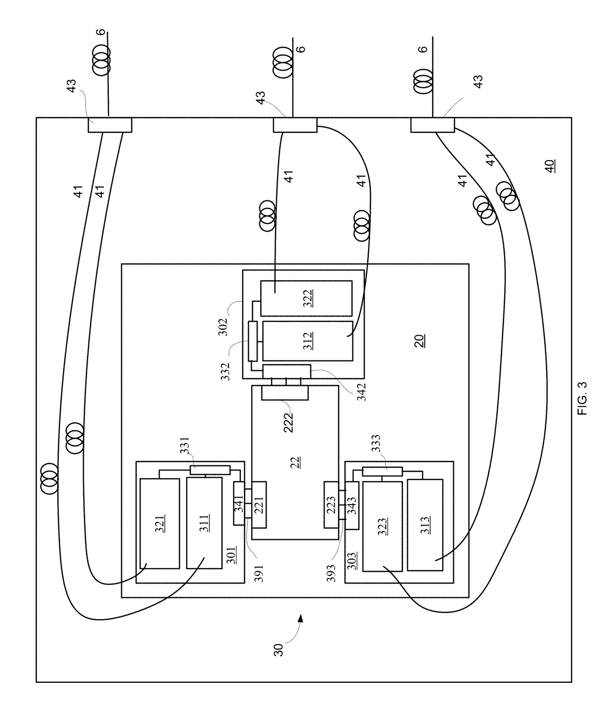
DETAILED DESCRIPTION OF THE DRAWINGS

[0052]In the following detailed description, numerous specific details are set forth in order to provide a thorough understanding of the invention. However, it will be understood by those skilled in the art that the present invention may be practiced without these specific details. In other instances, well-known methods, procedures, and components have not been described in detail so as not to obscure the present invention.

[0053]The subject matter regarded as the invention is particularly pointed out and distinctly claimed in the concluding portion of the specification. The invention, however, both as to organization and method of operation, together with objects, features, and advantages thereof, may best be understood by reference to the following detailed description when read with the accompanying drawings.

[0054]It will be appreciated that for simplicity and clarity of illustration, elements shown in the figures have not necessarily been drawn...


PUM


Abstract

A high-frequency optoelectronic module, that includes a first chip, a substrate and at least one optoelectronic unit. The first chip includes a set of high-frequency electrical IO interfaces. The at least one optoelectronic unit includes a group of high-frequency electrical IO interfaces and a group of high-frequency optical IO interfaces. The group of high-frequency optical IO interfaces is coupled to the group of high-frequency electrical IO interfaces. The substrate is coupled to the first chip and the at least one optoelectronic chip. The set of high-frequency electrical IO interfaces is coupled to the group of high-frequency electrical IO interfaces via a group of conductors. A length of each conductor of the group of conductors is of a scale that does not exceed a millimetric scale. The at least one optoelectronic circuit is configured to (a) convert high-frequency output electrical signals from the first chip to high-frequency output optical signals, and (b) convert high-frequency input optical signals sent towards the first chip to high-frequency input electrical signals. The high-frequency it not smaller than one hundred gigabits per second.

Description

BACKGROUND[0001]The ever-growing increase in global internet traffic imposes significant challenges on data center operators. An almost exponential growth is found for both intra- and inter-data center traffic originating from the continuous growth of cloud-based applications, social media and big data analytics. Modern data centers utilize hundreds of thousands of servers which require an efficient interconnection network which is both low-cost and energy-efficient.[0002]Network topology requires that all server nodes are connected to each one via a set of switches arranged in several hierarchy layers. Since the network is designed as a non-blocking Clos network, the number of switch ports must be large enough to support the entire data center traffic without any congestion created.[0003]As a result, the bandwidth of switches deployed doubles itself every 2-3 years with 12.8 Tera-bits per second (Tb / s) being the largest bandwidth in use today and 25.6 Tb / s scheduled to arrive by 20...

Claims


Application Information

Patent Timeline
IPC IPC(8): H04B10/80G02B6/42H04B10/25
CPCH04B10/801H04B10/2504G02B6/4279H04B10/40H04J14/0256G02B6/425G02B6/4214H04B10/25891
Inventor HASHARONI, JACOB
Owner DUST PHOTONICS LTD
Why Eureka
Try Eureka