Fabrication of a transistor with a channel structure and semimetal source and drain regions

a technology of semi-metal sources and transistors, applied in the field of microelectronics and semiconductors, can solve problems such as improving the structure of transistors

Active Publication Date: 2019-02-07
COMMISSARIAT A LENERGIE ATOMIQUE ET AUX ENERGIES ALTERNATIVES
View PDF5 Cites 0 Cited by
  • Summary
  • Abstract
  • Description
  • Claims
  • Application Information

AI Technical Summary

Problems solved by technology

The problem of improving such a transistor structure arises, in particular at the contact resistances with the source and drain regions.

Method used


Image

  • Fabrication of a transistor with a channel structure and semimetal source and drain regions
  • Fabrication of a transistor with a channel structure and semimetal source and drain regions
  • Fabrication of a transistor with a channel structure and semimetal source and drain regions

Examples


Embodiment Construction

[0004]The present invention relates to the fabrication of a transistor device with a vertically arranged channel and which is based on a semimetal such as bismuth, wherein the source and drain regions contact resistances are in particular reduced.

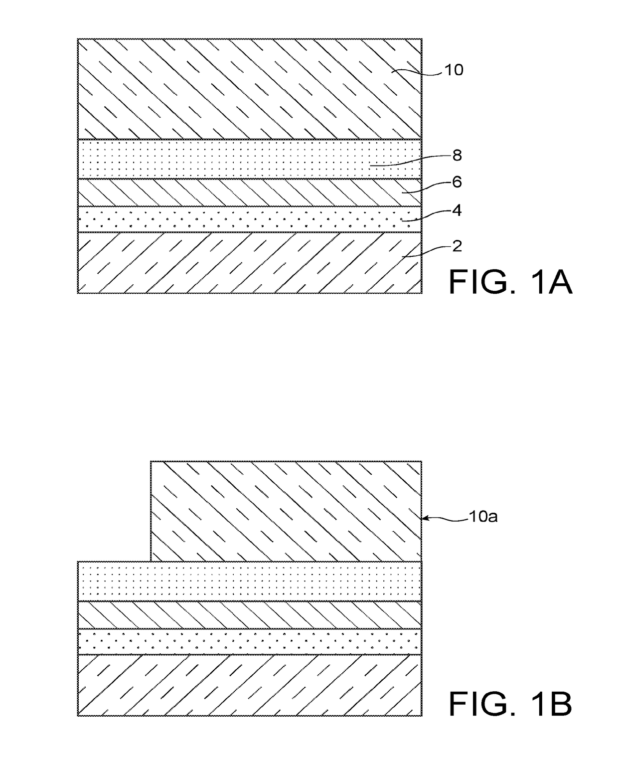
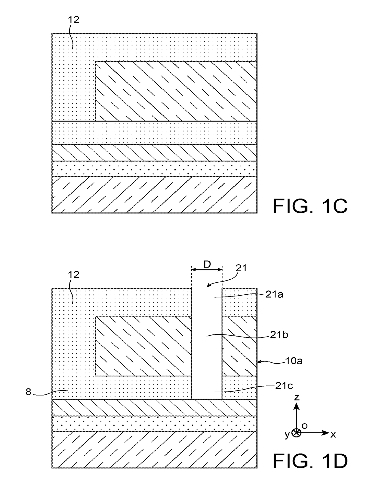
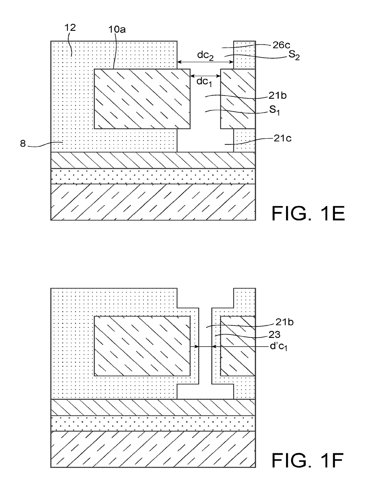
[0005]In order to do this, one embodiment of the present invention envisages a method comprising steps for:[0006]the formation of a stack equipped with a first source or drain contact zone and of a first layer on this first contact zone,[0007]the formation on this stack of a gate block and of a second layer on this gate block,[0008]the formation of at least one hole passing through the second layer, the gate block and the first layer so as to reveal the first contact zone, where the hole is made so as to have a first portion and a second portion located in the first layer and in the second layer respectively, each having a cross-section that is greater than that of a third portion of the hole located in the gate block,[0009]filling the hole...


PUM

PropertyMeasurementUnit
temperatureaaaaaaaaaa
thicknessaaaaaaaaaa
thicknessaaaaaaaaaa

Abstract

A vertical channel transistor comprising: a structure made of a given bismuth-based material which passes through a gate block where the structure comprises a channel region which extends through the gate block and source and drain regions on either side of the channel region and of the gate block, where the source and drain regions have a cross-section which is greater than the cross-section of the channel region (FIG. 1K).

Description

TECHNICAL FIELD AND PRIOR ART[0001]The present application relates to the field of microelectronics and of semiconductors, in particular that of transistors formed from a semimetal base, such as bismuth.[0002]Document US2017 / 0125554 A1 describes, for example, a transistor which has a channel structure made of bismuth and whose arrangement is vertical, that is, in a direction which is substantially parallel to a normal to a principal plane of the support on which the transistor is formed.[0003]The problem of improving such a transistor structure arises, in particular at the contact resistances with the source and drain regions.DESCRIPTION OF THE INVENTION[0004]The present invention relates to the fabrication of a transistor device with a vertically arranged channel and which is based on a semimetal such as bismuth, wherein the source and drain regions contact resistances are in particular reduced.[0005]In order to do this, one embodiment of the present invention envisages a method co...

Claims


Application Information

Patent Timeline
Patent Type & Authority Applications(United States)
IPC IPC(8): H01L29/737H01L29/06H01L29/423H01L29/08H01L29/78H01L21/02H01L21/441H01L21/762C30B23/02C30B29/40
CPCH01L29/7371H01L29/0676H01L29/42392H01L29/0847H01L29/7827H01L21/02636H01L21/441H01L21/76224C30B23/02C30B29/40B82Y10/00B82Y40/00H01L29/66439H01L29/775H01L29/12H01L29/24
Inventor COLINGE, JEAN-PIERRE
Owner COMMISSARIAT A LENERGIE ATOMIQUE ET AUX ENERGIES ALTERNATIVES
Why Eureka
Try Eureka