Module
a technology of resin layers and modules, applied in the field of modules with resin layers, can solve the problems of reducing the reliability of the semiconductor module b>100/b>, and achieve the effects of reducing the occurrence of air bubbles
- Summary
- Abstract
- Description
- Claims
- Application Information
AI Technical Summary
Benefits of technology
Problems solved by technology
Method used
Image
Examples
first embodiment
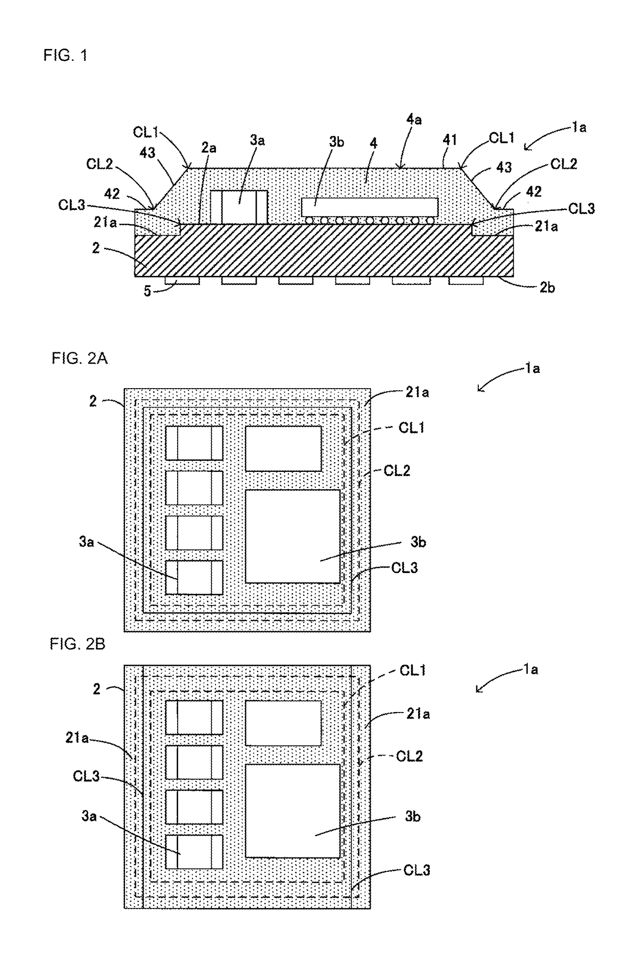
[0022]A module 1a according to a first embodiment of the present disclosure is described with reference to FIGS. 1 and 2. FIG. 1 is a cross-sectional view of the module 1a and FIGS. 2A and 2B are plan views of a wiring board 2 of the module 1a in FIG. 1.
[0023]As illustrated in FIG. 1, the module 1a according to the first embodiment of the present disclosure includes the wiring board 2, a plurality of components 3a and 3b mounted over an upper face 2a of the wiring board 2 (which corresponds to a principal face of a wiring board in the present disclosure), and a sealing resin layer 4 laminated over the upper face 2a of the wiring board 2, and is placed over a motherboard of an electronic apparatus for example.
[0024]The sealing resin layer 4 is laminated over the wiring board 2 so as to cover the upper face 2a of the wiring board 2 and each of the components 3a and 3b. On the upper face 4a, the sealing resin layer 4 includes a high-level region 41 with a long distance from the upper f...
second embodiment
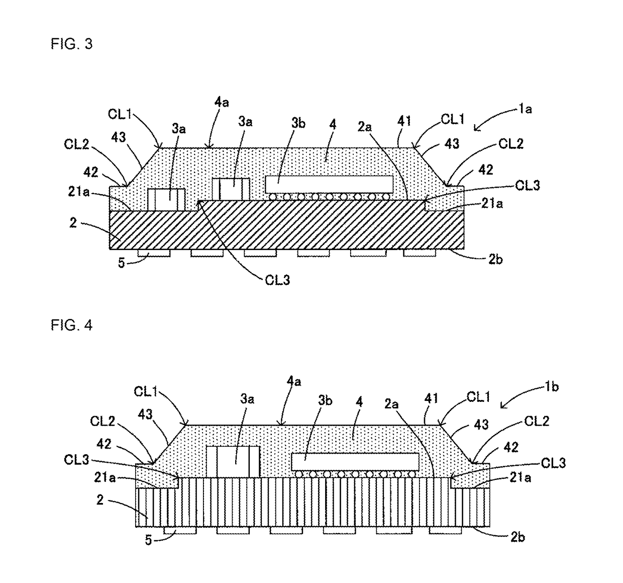
[0043]A module 1b according to a second embodiment of the present disclosure is described with reference to FIG. 4. FIG. 4 is a cross-sectional view of the module 1b.
[0044]The module 1b according to the present embodiment is different compared to the first embodiment described with reference to FIGS. 1 and 2 in that a wiring board 2 is a low temperature co-fired ceramics (LTCC) board as illustrated in FIG. 4. The other structures are the same as those of the module la in the first embodiment and the descriptions thereof are thus omitted by allocating the same reference signs.
[0045]As illustrated in FIG. 4, in the present embodiment, the wiring board 2 is formed from LTCC. Similar to the case in the first embodiment, mount electrodes (not illustrated) for mounting components 3a and 3b and a surface layer conductor (not illustrated) are formed on an upper face 2a of the wiring board 2 and outer electrodes 5 for external connection are formed on a lower surface 2b. In the present embo...
PUM
 Abstract
Description
Claims
Application Information


