
Quantum dot emitting diode and quantum dot display device including the same

a technology of emitting diodes and quantum dots, applied in the direction of solid-state devices, organic semiconductor devices, coatings, etc., can solve the problem of reducing the emitting efficiency of qd emitting diodes, and achieve the effect of improving the charge balan

Pending Publication Date: 2019-03-14
LG DISPLAY CO LTD
View PDF8 Cites 14 Cited by
  • Summary
  • Abstract
  • Description
  • Claims
  • Application Information

AI Technical Summary

Benefits of technology

This patent aims to improve the charge balance of a QD emitting diode and a QD display device. The technical effect of this innovation is to enhance the efficiency and performance of the device, leading to better display quality and reduced power consumption.

Problems solved by technology

However, in the related art QD emitting diode, the charge balance is destroyed such that the emitting efficiency of the QD emitting diode is decreased.

Method used


Image

  • Quantum dot emitting diode and quantum dot display device including the same
  • Quantum dot emitting diode and quantum dot display device including the same
  • Quantum dot emitting diode and quantum dot display device including the same

Examples


example 1

2. Example 1

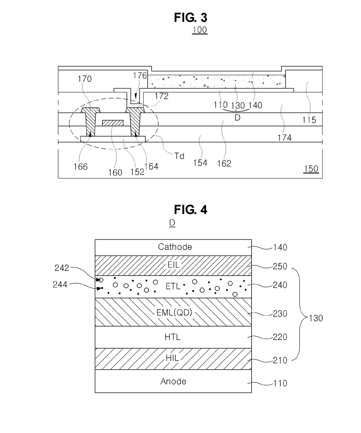
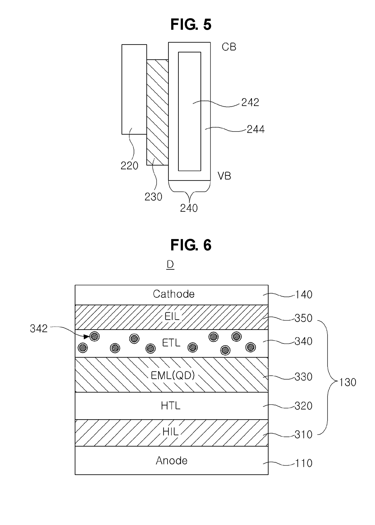
[0132]ZnO (7˜8 nm)-SiO2 (2˜3 nm) particle (core-shell) is used as the electron transporting material.

example 2

3. Example 2

[0133]ZnMgO (7˜8 nm)-SiO2 (2˜3 nm) particle (core-shell) is used as the electron transporting material.

example 3

4. Example 3

[0134]SnO2 (7˜8 nm)-SiO2 (2˜3 nm) particle (core-shell) is used as the electron transporting material.

[0135]FIGS. 9A to 9D are graphs showing an emission peak of the QD emitting diode including the electron transporting material with or without a silica shell.

[0136]When the ZnO electron transporting material without a silica shell is used to the ETL, the balance between the hole and the electron is destroyed such that the emission may be generated at the interface between the ETL and the QD EML. Namely, as shown in FIG. 9A, not only the emission peak by the QD but also the emission peak by the hole transporting material (TFB) is detected.

[0137]However, when the core-shell structure electron transporting material is used to the ETL (Examples 1 to 3), the emission peak by the hole transporting material is not detected such that the emission property of the QD emitting diode is improved. (FIGS. 9B to 9D)

[0138]FIGS. 10A to 10C are graphs showing an emitting efficiency of the...


PUM

PropertyMeasurementUnit
Thicknessaaaaaaaaaa
Thicknessaaaaaaaaaa
Sizeaaaaaaaaaa

Abstract

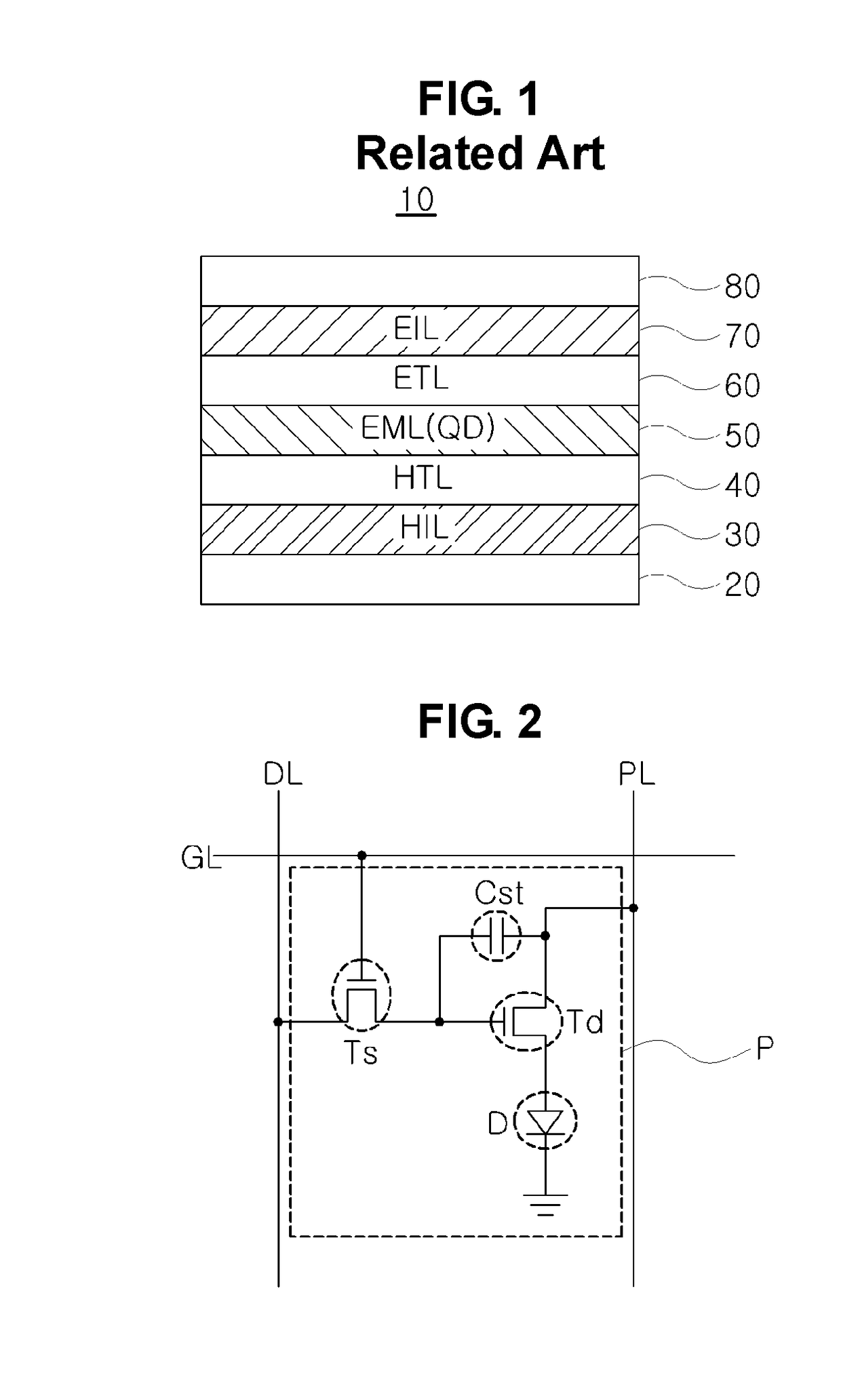
A quantum dot emitting diode includes first and second electrodes facing each other; a quantum dot emitting material layer between the first and second electrodes; and an electron transporting layer including an electron transporting material and disposed between the quantum dot emitting material layer and the second electrode, wherein the electron transporting material includes a core of metal oxide and a shell of silica.

Description

CROSS-REFERENCE TO RELATED APPLICATIONS[0001]The present application claims the benefit of Korean Patent Application No. 10-2017-0116500 filed in the Republic of Korea on Sep. 12, 2017, and Korea Patent Application No. 10-2018-0107719 filed on Sep. 10, 2018, all of which are hereby incorporated by reference in their entirety into the present application.BACKGROUNDTechnical Field[0002]The present disclosure relates to a quantum dot (QD) emitting diode, and more particularly, to a QD emitting diode having improved charge balance and a QD display device including the same.Discussion of the Related Art[0003]As information technology and mobile communication technology have been developed, a display device being capable of displaying a visual image has also been developed. Flat panel display devices, such as a liquid crystal display (LCD) device a plasma display panel (PDP) device and an electroluminescent display device, are developed and used because of advantages in weight, power cons...

Claims


Application Information

Patent Timeline
IPC IPC(8): H01L51/50H01L51/52H01L27/32C08L29/04C08K3/36C08K3/22
CPCH01L51/502H01L51/5092H01L51/5206H01L51/5221H01L27/3262C08L29/04C08K3/36C08K3/22H01L51/5076H01L51/5056C08L2207/53C08K2003/2296C08K2003/2217C08K2003/2231H10K59/12H10K50/115H10K50/16H10K2102/102H10K2102/103C09D129/04H10K50/165H10K2102/331H10K2102/351H10K50/81H10K50/82H10K50/171H10K59/1213H10K50/15
Inventor KIM, MIN-JEEWOO, SUNG-ILCHOI, HYE-OCKKANG, JI-YEON
Owner LG DISPLAY CO LTD
Learn More