Nano-tube mosfet technology and devices

Active Publication Date: 2016-11-03
ALPHA & OMEGA SEMICON INC
View PDF1 Cites 5 Cited by
  • Summary
  • Abstract
  • Description
  • Claims
  • Application Information

AI Technical Summary

Benefits of technology

[0016]It is therefore an aspect of the present invention to provide a new and improved device structure and manufacturing method to form the doped columns in the drift regions for charge balance with simple and convenient processing steps. The simplified processes are achieved through stacking multiple epitaxial layers formed as nano-tubes by etching trenches with larger openings that is about five to ten microns or more surrounding pillar columns of about three to five microns. Epitaxial layers with varying thicknesses ranging from a few microns to less than one micron are grown with alternating N and P type dopants constituting nano tubes to fill the trenches with a central gap less than a width set for a particular filling process (about a micron or less for most cases). Then the central gap can be filled with a gap filling layer which may be insulating such as thermally

Problems solved by technology

The remaining gap may be filled as center nano tube, but this may be very

Method used


Image

  • Nano-tube mosfet technology and devices
  • Nano-tube mosfet technology and devices
  • Nano-tube mosfet technology and devices

Examples


Embodiment Construction

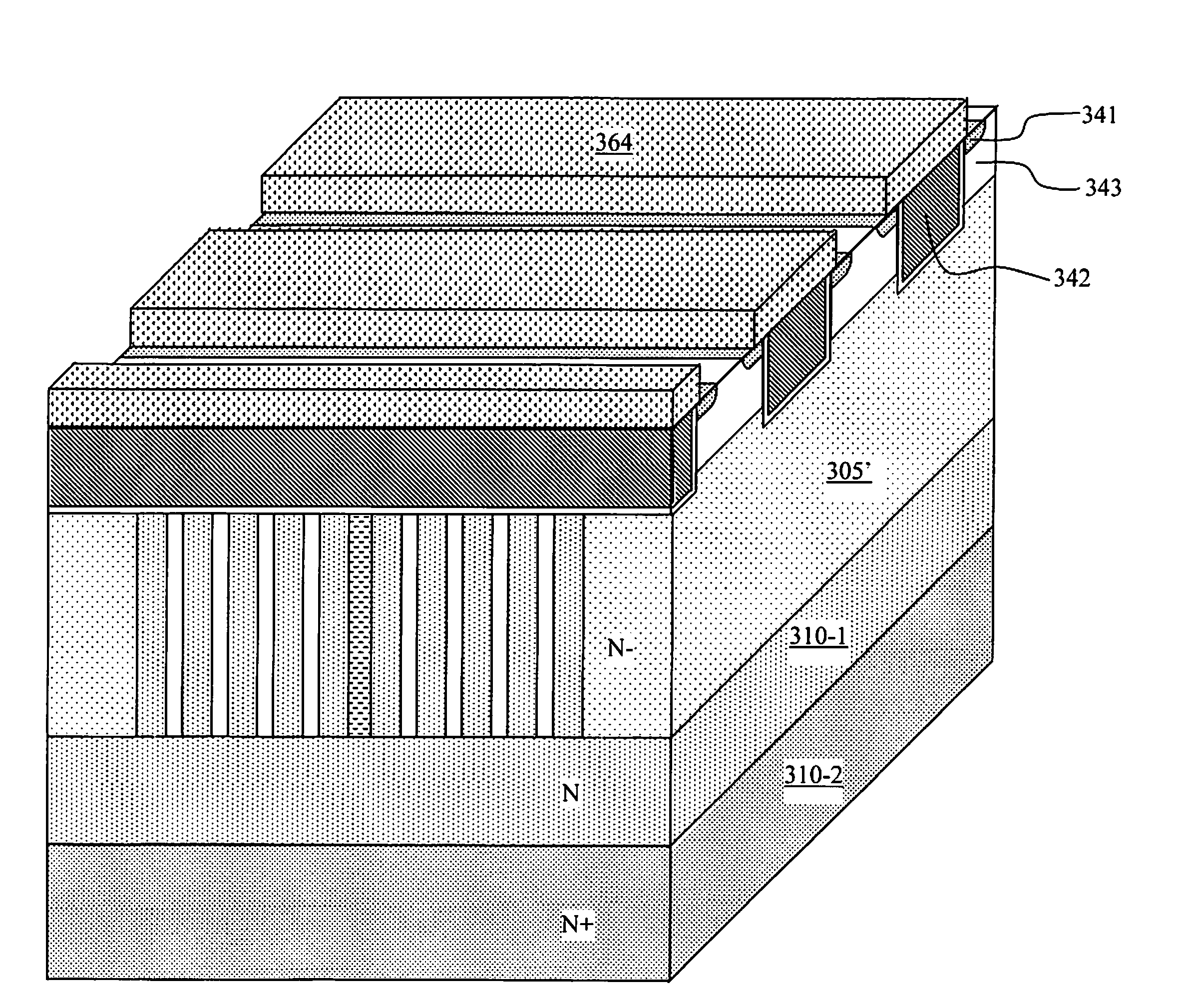
[0063]Referring to FIG. 2 for a cross sectional view of a unit cell 101 of a vertical nano-tube high-voltage (HV) diode device 100 that illustrates the new concepts including the new structural and manufacturing features of this invention. The HV diode device 100 is supported on a heavily doped N type bottom substrate 105, e.g., an N+ red phosphorous substrate, which lies below an N+, nano tube merger region 105-B which may be a diffusion bottom region 105-B and an N+ column diffusion region 105-C, which may be formed by a diffusion process as will be described below. The HV device further includes a plurality of N-type nano tubes and P-type nano tubes formed as N-type thin epitaxial layers 115-N and P-type thin epitaxial layers 115-P. These nano-tubes are formed as alternating N-epitaxial layers 115-N and P-epitaxial layers 115-P between two P-type pillars 110 as vertical nano-tubes extended from a P-implant top-layer 130 to the bottom N+ region 105-B. The HV nano-tube diode device...


PUM


Abstract

This invention discloses a semiconductor power device disposed in a semiconductor substrate and the semiconductor substrate has a plurality of trenches. Each of the trenches is filled with a plurality of epitaxial layers of alternating conductivity types constituting nano tubes functioning as conducting channels stacked as layers extending along a sidewall direction with a “Gap Filler” layer filling a merging-gap between the nano tubes disposed substantially at a center of each of the trenches. The “Gap Filler” layer can be very lightly doped Silicon or grown and deposited dielectric layer. In an exemplary embodiment, the plurality of trenches are separated by pillar columns each having a width approximately half to one-third of a width of the trenches.

Description

[0001]This patent application is a Divisional application of a co-pending application Ser. No. 13 / 594,837 filed on Aug. 26, 2012. Application Ser. No. 13 / 594,837 is a Continuation application of another application Ser. No. 13 / 065,880 filed on Mar. 31, 2011 now issued into U.S. Pat. No. 8,263,482. Application Ser. No. 13 / 065,880 is a Divisional application of another application Ser. No. 12 / 319,164 filed on Dec. 31, 2008 now issued into U.S. Pat. No. 7,943,989. The Disclosures made in the patent application Ser. No. 12 / 319,164, application Ser. No. 13 / 065,880 and application Ser. No. 13 / 594,837 are hereby incorporated by reference in this patent application.BACKGROUND OF THE INVENTION[0002]1. Field of the Invention[0003]The invention relates generally to the semiconductor power devices. More particularly, this invention relates to configurations and methods implemented with alternating doped nano-tubes for manufacturing flexibly scalable charge balanced semiconductor power devices w...

Claims


Application Information

Patent Timeline
IPC IPC(8): H01L29/06H01L21/306H01L29/08H01L29/66H01L29/10
CPCH01L29/0696H01L29/66712H01L29/1095H01L21/30625H01L29/0865H01L29/0676H01L29/0882H01L29/0634H01L29/0649H01L29/0821H01L29/0878H01L29/66734H01L29/7371H01L29/7395H01L29/7397H01L29/7802H01L29/7811H01L29/7813H01L29/8083H01L29/861H01L29/872H01L29/66893
Inventor YILMAZ, HAMZANG, DANIELGUAN, LINGPINGBHALLA, ANUPMA, WILSONHO, MOSESCHEN, JOHN
Owner ALPHA & OMEGA SEMICON INC
Why Eureka
Try Eureka