High voltage structures and methods for vertical power devices with improved manufacturability

a technology of vertical power devices and structures, applied in the direction of semiconductor devices, basic electric elements, electrical apparatus, etc., can solve the problems of low yield, low throughput of high-voltage semiconductor power devices, and difficulty in conventional manufacturing technologies and device configurations to further increase breakdown voltage with reduced series resistance, etc., to achieve convenient manufacturing, reduce processing steps, and reduce processing steps

Inactive Publication Date: 2009-07-02
ALPHA & OMEGA SEMICON LTD
View PDF4 Cites 29 Cited by
  • Summary
  • Abstract
  • Description
  • Claims
  • Application Information

AI Technical Summary

Benefits of technology

[0010]It is therefore an aspect of the present invention to provide a new and improved device structure and manufacturing method to form the doped columns in the drift regions for charge balance with simple and convenient processing steps achieved through doping trench sidewalls of deep trenches that do not extend through the entire vertical drift region. There are no etch-back or CMP (chemical mechanical polishing) required thus reducing the processing steps and can be implemented with just few and thin epitaxial growth such as two epitaxial layers less than fifteen micrometers thickness for each layer. The manufacturing processes required a few staged trenches with reasonable aspect ratio, e.g., two staged trenches less than 15 microns with aspect ratio of approximately 5:1. The device can be conveniently manufactured with standard processing using standard processing modules and equipment. Therefore, the above discussed technical difficulties and limitations can be resolved.

Problems solved by technology

Conventional manufacturing technologies and device configuration to further increase the breakdown voltage with reduced series resistance are still confronted with manufacturability difficulties.
The practical applications and usefulness of the high voltage semiconductor power devices are limited due to the facts that the conventional high power devices generally have structural features that require numerous time-consuming, complex, and expensive manufacturing processes.
Some of the processes for manufacturing the high voltage power devices have low throughput and low yields.
Specifically, multiple epitaxial layers and buried layers are required in some of the conventional structures and some devices require very deep trenches, which require a long time to etch.
Furthermore, the manufacturing processes often require equipment not compatible with standard foundry processes.
Additionally, these devices have structural features and manufacturing processes not conducive to scalability for low to high voltage applications.
In other words, some approaches would become too costly and / or too lengthy to be applied to higher voltage ratings.
As will be further reviewed and discussions below, these conventional devices with different structural features and manufactured by various processing methods, each has limitations and difficulties that hinder practical applications of these devices as now demanded in the marketplace.
Despite the advantages that the devices can be manufactured with simple processes and low manufacturing cost, these devices are however not feasible for high current low resistance applications in the standard packages due the above discussed drawbacks: the die cost becomes prohibitive (because there are too few dies per wafer) and it becomes impossible to fit the larger die in the standard accepted packages.
The floating island structure is limited by the technical difficulties due to charge storage and switching issues.
The conventional device structures of class-one type devices as discussed above still have limitations that such devices require die of large size to achieve a low Rdson resistance.
Due to the size issue, it is usually not feasible to achieve low Rdson and high current application by using standard power packages.
For class-two and class-three types of devices, the manufacture methods are generally very complex, expensive and require long processing time due to the facts that the methods require multiple steps and several of these steps are slow and having a low throughput.
For these reasons, the conventional structures and manufacture methods are limited by slow and expensive manufacturing processes and are not economical for broad applications.

Method used


Image

  • High voltage structures and methods for vertical power devices with improved manufacturability
  • High voltage structures and methods for vertical power devices with improved manufacturability
  • High voltage structures and methods for vertical power devices with improved manufacturability

Examples


Embodiment Construction

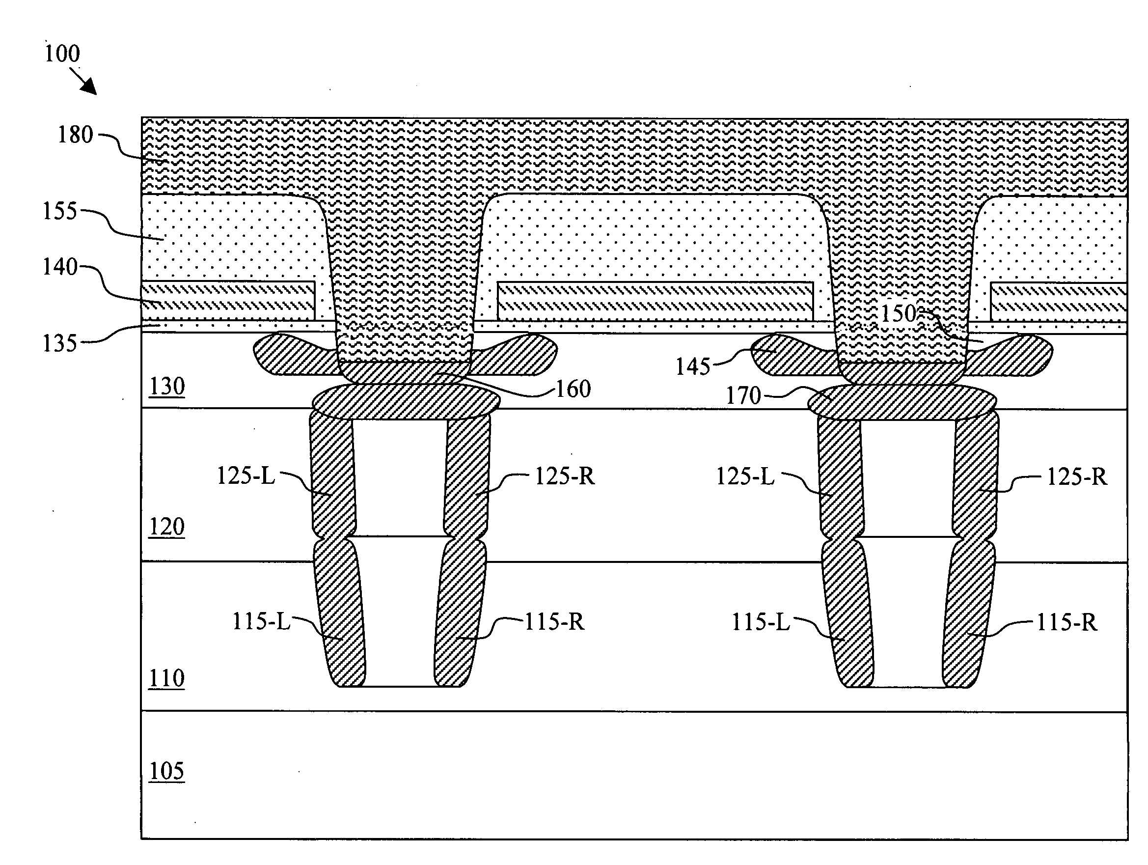
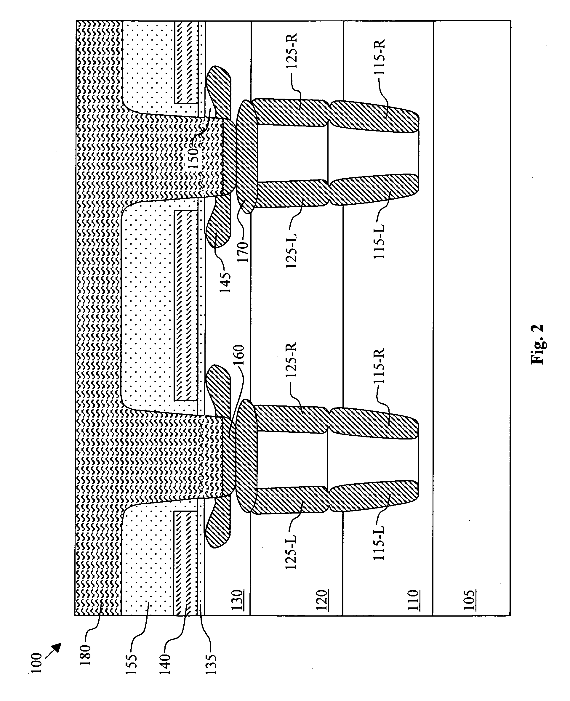
[0024]Referring to FIG. 2 for a cross sectional view of a planar MOSFET device 100 of this invention. The MOSFET device 100 is supported on an N+ silicon substrate 105 functioning as a drain terminal or electrode on a bottom surface of the substrate. The N+ substrate 105 supports a N-drift region 110 formed immediately on top of the N+ drain region 105 with a first N-epitaxial layer 120 on top of the drift region 110 and a second N-epitaxial layer 130 formed on top of the first N-epitaxial layer 120. The N-drift layer 110 includes bottom P-doped columns 115 and the first N-epitaxial layer 120 includes top P-doped columns 125. As will be further described below, the bottom P-doped columns 115 are formed by applying tilt angle P-dopant ion implantation through the sidewalls the trenches opened between two adjacent P-doped columns 115-L and 115-R. In this embodiment, compensation implant in the form of a zero tilt N-type implant (Phosphorus for example) is performed to compensate any o...


PUM


Abstract

This invention discloses a semiconductor power device disposed on a semiconductor substrate supporting an epitaxial layer as a drift region composed of an epitaxial layer. The semiconductor power device further includes a super-junction structure includes a plurality of doped sidewall columns disposed in a multiple of epitaxial layers. The epitaxial layer have a plurality of trenches opened and filled with the multiple epitaxial layer therein with the doped columns disposed along sidewalls of the trenches disposed in the multiple of epitaxial layers.

Description

BACKGROUND OF THE INVENTION[0001]1. Field of the Invention[0002]The invention relates generally to the vertical semiconductor power devices. More particularly, this invention relates to configurations and methods with improved manufacturability for manufacturing vertical semiconductor power devices with a super-junction structure for high voltage applications.[0003]2. Description of the Prior Art[0004]Conventional manufacturing technologies and device configuration to further increase the breakdown voltage with reduced series resistance are still confronted with manufacturability difficulties. The practical applications and usefulness of the high voltage semiconductor power devices are limited due to the facts that the conventional high power devices generally have structural features that require numerous time-consuming, complex, and expensive manufacturing processes. Some of the processes for manufacturing the high voltage power devices have low throughput and low yields. Specific...

Claims


Application Information

Patent Timeline
Patent Type & Authority Applications(United States)
IPC IPC(8): H01L29/78H01L21/336
CPCH01L21/26586H01L29/0634H01L29/0878H01L29/7802H01L29/41766H01L29/66727H01L29/1095
Inventor HEBERT, FRANCOIS
Owner ALPHA & OMEGA SEMICON LTD
Why Eureka
Try Eureka