Super junction device and manufacturing method thereof

A superjunction device, N-type technology, applied in semiconductor/solid-state device manufacturing, semiconductor devices, electrical components, etc., can solve the problems of poor device EAS capability, poor BVds consistency, and insufficient BVds effect.

Active Publication Date: 2019-05-14
SHENZHEN SANRISE TECH CO LTD
View PDF8 Cites 6 Cited by
  • Summary
  • Abstract
  • Description
  • Claims
  • Application Information

AI Technical Summary

Problems solved by technology

But the problem is that even if the N-type epitaxial layer is made into two layers, the concentration of the upper half is high and the concentration of the lower half is low, but in this way, there will still be significantly more N-type impurities than P-type impurities in the bottom area of ​​the trench. P-N balance, thus affecting BVds
Another problem is that due to the increase in the concentration of the N-type epitaxy at the top of the terminal region, the ability of the terminal region to withstand voltage laterally is reduced, resulting in device breakdown occurring in the terminal region, which not only fails to improve the effect of BVds, but also due to BVds Occurs at the terminal, making the consistency of BVds worse, and the EAS capability of the device is also worse

Method used


Image

  • Super junction device and manufacturing method thereof
  • Super junction device and manufacturing method thereof
  • Super junction device and manufacturing method thereof

Examples


no. 1 example approach

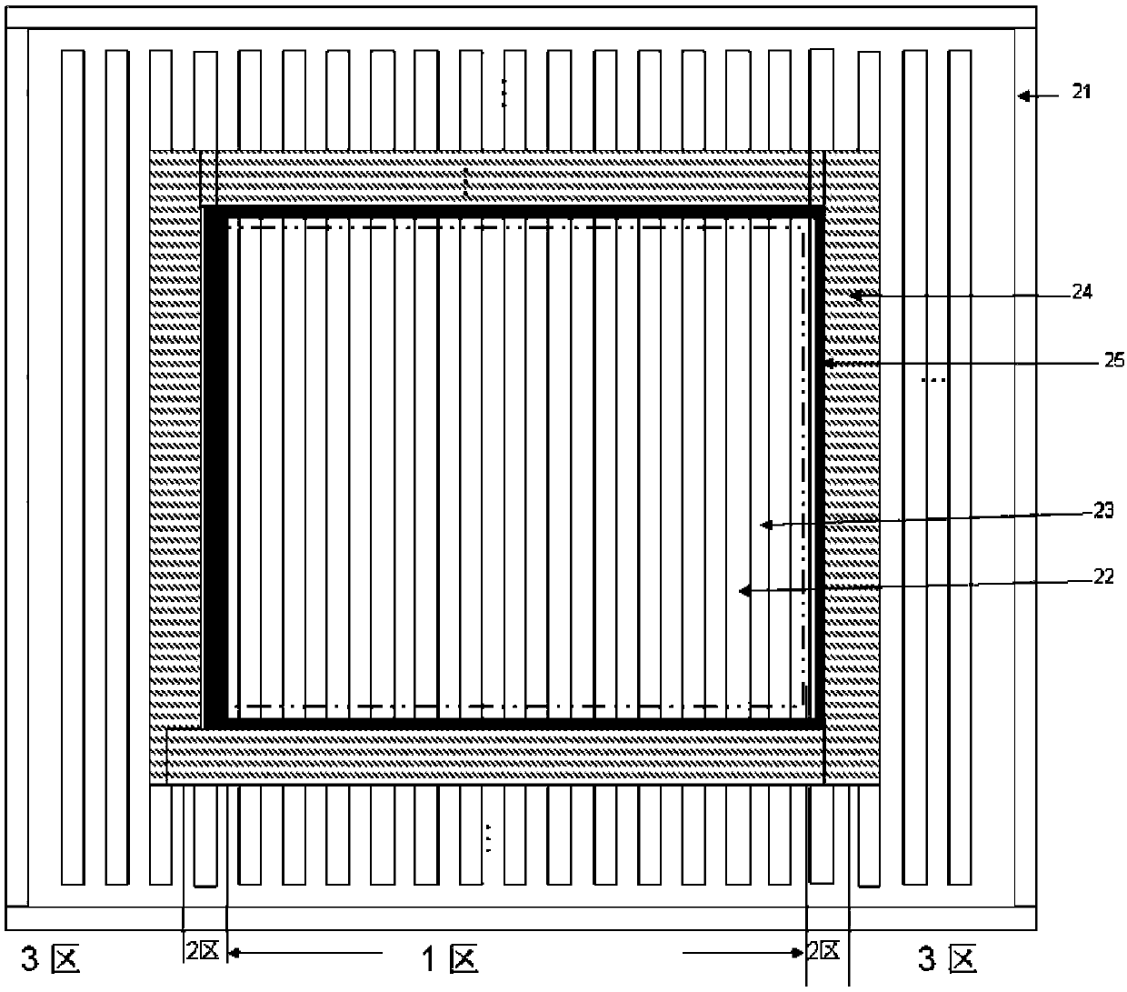
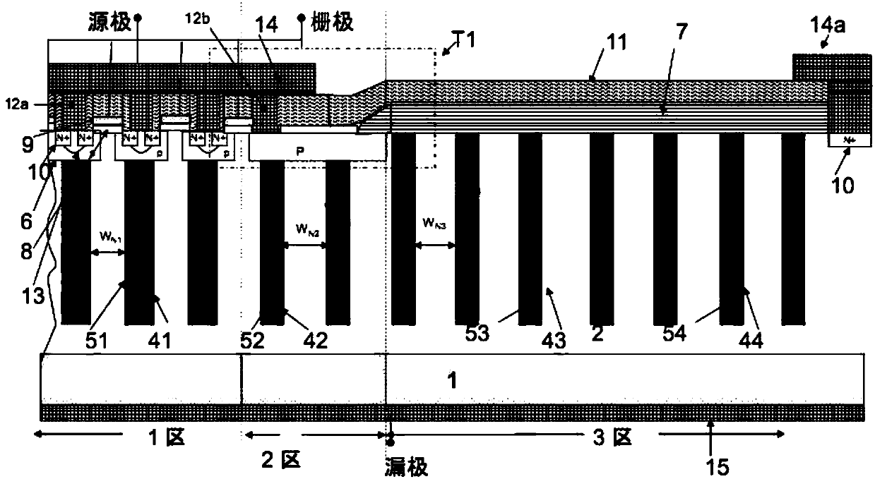
[0143] The manufacturing method of the super junction device according to the first embodiment of the present invention is to manufacture such as image 3 The superjunction device of the embodiment of the present invention is shown as an example for description, as Figure 5A to Figure 5H Shown is a schematic cross-sectional view of the device in each step of the manufacturing method of the super-junction device in the first embodiment of the present invention; in the manufacturing method of the super-junction device in the first embodiment of the present invention, the middle region of the super-junction device is the current flow region, that is, 1 zone, the terminal zone, that is, zone 3, surrounds the periphery of the current flow region, and the transition zone, that is, zone 2, is located between the current flow zone and the terminal zone; the structure of the top view of the super junction device can also refer to figure 1 shown. The method of the first embodiment of ...

no. 1 example

[0163] A P-type well 6 is formed on the top of each P-type column 51 in the current flow region, and each P-type well 6 extends to the N-type well 6 on both sides of the corresponding P-type column 51. surface of the column. In the method of the first embodiment of the present invention, one P-type well 6 is formed in the second region, and the P-type well 6 covers the two P-type pillars 52.

[0164] After the P-type ion implantation of the P-type well 6 is completed, it also includes performing an annealing process on the P-type well 6. The temperature of the annealing process is above 1000°C and the time is above 30 minutes.

[0165] In the method of the first embodiment of the present invention, the process conditions of the P-type well 6 need to meet the requirements of the threshold voltage of the device. For devices with a threshold voltage requirement of 2 volts to 4 volts, B 30-100KEV, 3-10 E13 can be used / cm2 process conditions, that is, the implanted impurity is bo...
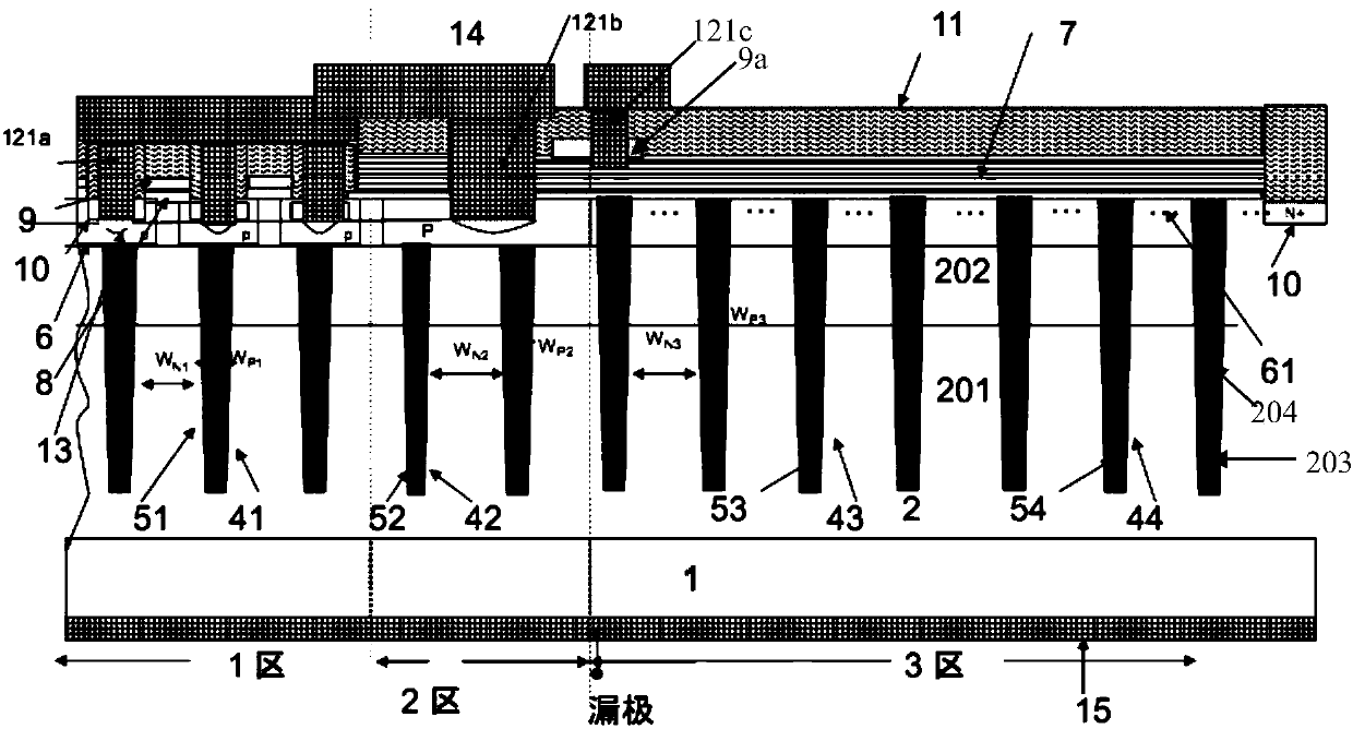
no. 2 example

[0214] A P-type well 6 is formed on the top of each P-type column 51 in the current flow region, and each P-type well 6 extends to the N-type well 6 on both sides of the corresponding P-type column 51. surface of the column. In the method of the second embodiment of the present invention, one P-type well 6 is formed in the second region, and the P-type well 6 covers the two P-type pillars 52.

[0215] After the P-type ion implantation of the P-type well 6 is completed, it also includes performing an annealing process on the P-type well 6. The temperature of the annealing process is above 1000°C and the time is above 30 minutes.

[0216] In the method of the second embodiment of the present invention, the process conditions of the P-type well 6 need to meet the requirements of the threshold voltage of the device. For devices with a threshold voltage requirement of 2 volts to 4 volts, B 30-100KEV, 3-10E13 / cm2 process conditions, that is, the implanted impurity is boron (B), th...


PUM


Abstract

The invention discloses a super junction device, grooves of a super junction structure are of a lateral inclined structure, the doping concentration of N-type epitaxial layers are distributed in a stepped mode, and P-type columns are formed of a plurality of layers of P-type epitaxial layers which are filled in the grooves in an overlapped mode; and the doping concentration of the P-type epitaxiallayers of the P-type columns is decreased successively from bottoms to tops of the grooves. A protective epoxy film wraps around the circumferential side of a current flow region; and the N-type epitaxial layer at the interface of the protective epoxy film and the oxide film epitaxial layer of the N-type epitaxial layer of a terminal region internally comprises a top region with the reduced N-type doping concentration, and the top region can enhance the lateral depletion capacity of the N-type column at the interface of the oxide film epitaxial layer. The invention further discloses a manufacturing method of the super junction device. According to the super junction device, the charge balance between the P-type columns and N-type columns of the super junction structure with the inclined grooves can be improved, the longitudinal voltage endurance capability of the device is improved, and the source leakage breakdown voltage of the device is increased; and the lateral voltage bearing capacity of a device terminal can further be improved, and reliability of the device is improved.

Description

technical field [0001] The invention relates to a method for manufacturing a semiconductor integrated circuit, in particular to a method for manufacturing a superjunction device. Background technique [0002] The super junction structure is composed of alternately arranged N-type pillars and P-type pillars. If the superjunction structure is used to replace the N-type drift region in the vertical double-diffused MOS transistor (Vertical Double-diffused Metal-Oxide-Semiconductor, VDMOS) device, the conduction path is provided through the N-type column in the conduction state, and when the conduction The P-type column does not provide a conduction path; in the off state, the PN column jointly bears the reverse bias voltage, forming a super-junction metal-oxide-semiconductor field-effect transistor (Metal-Oxide-Semiconductor Field-Effect Transistor, MOSFET). The super junction MOSFET can greatly reduce the on-resistance of the device by using a low-resistivity epitaxial layer w...

Claims


Application Information

Patent Timeline
Patent Type & Authority Applications(China)
IPC IPC(8): H01L29/06H01L29/78H01L21/336
Inventor 肖胜安
Owner SHENZHEN SANRISE TECH CO LTD
Why Eureka
Try Eureka