Silicon-on-insulator flat panel display driver chip and preparation method thereof

A display driver and chip technology, applied in semiconductor/solid-state device manufacturing, electric solid-state devices, semiconductor devices, etc., can solve problems affecting chip performance and reliability, affecting device reliability, occupying chip area, etc., to achieve good reliability performance , low chip power consumption, and the effect of improving the vertical withstand voltage level

Active Publication Date: 2012-02-01
SOUTHEAST UNIV
View PDF0 Cites 0 Cited by
  • Summary
  • Abstract
  • Description
  • Claims
  • Application Information

AI Technical Summary

Problems solved by technology

However, in the traditional bulk silicon or buried layer process, in order to achieve a high voltage of more than 100V, the thickness of the external lamination layer is relatively high. At the same time, the substrate leakage current will increase the power consumption of the device due to the connection between the substrate and the device, and will affect the device. reliability, which in turn affects the performance and reliability of the entire chip; and the traditional high-voltage device isolation methods are mainly single-slot filled silicon dioxide and polysilicon isolation, deep junction isolation and pn junction self-isolation, these isolation methods take up a lot The proportion of the chip area, especially the pn junction isolation method, the area of ​​the chip used for isolation is more than 20%.

Method used


Image

  • Silicon-on-insulator flat panel display driver chip and preparation method thereof
  • Silicon-on-insulator flat panel display driver chip and preparation method thereof
  • Silicon-on-insulator flat panel display driver chip and preparation method thereof

Examples


Embodiment 1

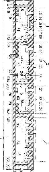
[0023] Below in conjunction with accompanying drawing, structure of the present invention is described in detail, as figure 1As shown, a flat panel display driver chip includes a P-type substrate 9, a buried oxide layer 7 is provided on the P-type substrate 9, and a high-voltage P-type lateral metal oxide semiconductor transistor 1 is provided on the buried oxide layer 7. The high-voltage N-type lateral metal oxide semiconductor transistor 2, the high-voltage diode 3, and the low-voltage device 4 are characterized in that the high-voltage P-type lateral metal oxide semiconductor transistor 1 is adjacent to the high-voltage N-type lateral metal oxide semiconductor transistor 2 and the high-voltage P-type lateral The drain terminal of the metal oxide semiconductor transistor 1 is adjacent to the source terminal of the high-voltage N-type lateral metal-oxide semiconductor transistor 2, and the high-voltage diode 3 is located between the high-voltage N-type lateral metal-oxide semi...

Embodiment 2

[0031] The preparation method of display driver chip of the present invention is as follows:

[0032] The first step: take the impurity concentration as 1.0e15cm -3 The P-type substrate 9 shown in Figure 2 (a) is pre-cleaned; the buried oxide layer 7 is prepared on the P-type substrate 9 as shown in Figure 2 (b); then the N-type impurity concentration is 1.5 e15cm -3 The epitaxial layer 8, while passing a dose of 3e13cm -2 boron ion implantation, on the N-type epitaxial layer 8 to make the first P-type heavily doped buried layer 10, the second P-type heavily doped buried layer 26 and the third P-type heavily doped buried layer 29, the passing dose is 3e12cm -2 The arsenic ion implantation forms the N-type buried layer 27 of the high-voltage N-type lateral metal oxide semiconductor transistor 2 and the N-type buried layer 28 of the high-voltage diode 3 as shown in Figure 2 (c); on the N-type epitaxial layer 8, a high-voltage N The P-type body region 25 of the N-type lateral ...


PUM


Abstract

Display driver chip composed of high-voltage P-type lateral metallic oxide transistors, high-voltage N-type lateral metallic oxide transistors, high-pressure diodes and low-voltage devices, among the high-voltage devices and between the high-voltage and low-voltage devices are separated by double-groove filled with silicon dioxide that extending from a buried oxide layer through a N-type epitaxial layer to a field oxide layer on device surface, partial N-type or P-type heavily dosed buried layer are disposed above the buried oxide layer that positioning under the N-type lateral metallic oxide transistors and the high-pressure diodes. The prepartion method is: preparing a buried oxide layer on a P-type substrate, preparing partial N-type or P-type heavily dosed buried layer above the buried oxide layer, depositing a N-type epitaxial layer, preparing high-voltage P-wells for high-voltage N-type lateral metallic oxide transistors and high-pressure diodes, preparing P-type drift region for high-voltage N-type lateral metallic oxide transistors, then preparing buffer layer of high-voltage tubes, lower-voltage wells of lower-voltage devices, contact holes of source drain region, evaporating aluminum, carving aluminum reversely and forming electrodes and metallic field panel, passivation.

Description

technical field [0001] The invention relates to a display driver chip and a preparation method thereof, and is especially suitable for a row address driver chip and a column address driver chip for a plasma display (PDP). Background technique [0002] The plasma display driver chip is mainly composed of a low-voltage complementary lateral metal-oxide-semiconductor logic circuit controlling a high-voltage device output circuit. Although the size of the display screen is increasing, the chip that actually controls the display is developing towards a highly integrated, smaller size, higher frequency, lower power consumption, better performance, and lower cost. Since the low-voltage complementary lateral metal-oxide-semiconductor technology is basically mature and the power consumption is very low, the improvement of the overall performance of the driver chip is mainly focused on the design and process of the power device in addition to the improvement of the circuit level. At ...

Claims


Application Information

Patent Timeline
Patent Type & Authority Patents(China)
IPC IPC(8): H01L27/12H01L29/06H01L21/84H01L21/76H01J17/49
Inventor 孙伟锋陈越政钱钦松夏晓娟吴虹时龙兴
Owner SOUTHEAST UNIV
Why Eureka
Try Eureka