Double-gate graphene transistor with silicon substrate and aluminium oxide gate dielectric, and preparation method

A technology of aluminum oxide and graphene, which is applied in the direction of transistors, semiconductor/solid-state device manufacturing, semiconductor devices, etc., can solve problems such as growth, affecting device performance, and inability to play an insulating role, so as to improve modulation and simplify production process, the effect of suppressing the scattering effect

Active Publication Date: 2014-05-21
XIDIAN UNIV
View PDF3 Cites 4 Cited by
  • Summary
  • Abstract
  • Description
  • Claims
  • Application Information

AI Technical Summary

Problems solved by technology

When its thickness is reduced to the nanometer level, through SiO 2 The leakage current increases exponentially as the thickness decreases, such a huge leakage current seriously affects the device performance, making SiO 2 Can not play an insulating role, eventually resulting in SiO 2 No longer suitable as gate dielectric for field effect transistor FET

Method used


Image

  • Double-gate graphene transistor with silicon substrate and aluminium oxide gate dielectric, and preparation method
  • Double-gate graphene transistor with silicon substrate and aluminium oxide gate dielectric, and preparation method
  • Double-gate graphene transistor with silicon substrate and aluminium oxide gate dielectric, and preparation method

Examples


Embodiment 1

[0038] Step 1: Clean the Si substrate sample to remove surface contaminants such as Figure 4 (a) shown.

[0039] (1.1) Use NH on the Si substrate sample 4 OH+H 2 o 2 Soak the sample in the reagent for 10 minutes, take it out and dry it to remove the organic residue on the surface of the sample;

[0040] (1.2) Use HCl+H on the Si substrate sample after removing the surface organic residues 2 o 2 Soak the sample in the reagent for 10 minutes, take it out and dry it to remove ionic pollutants.

[0041] Step 2: Grow the carbonized layer, such as Figure 4 (b) shown.

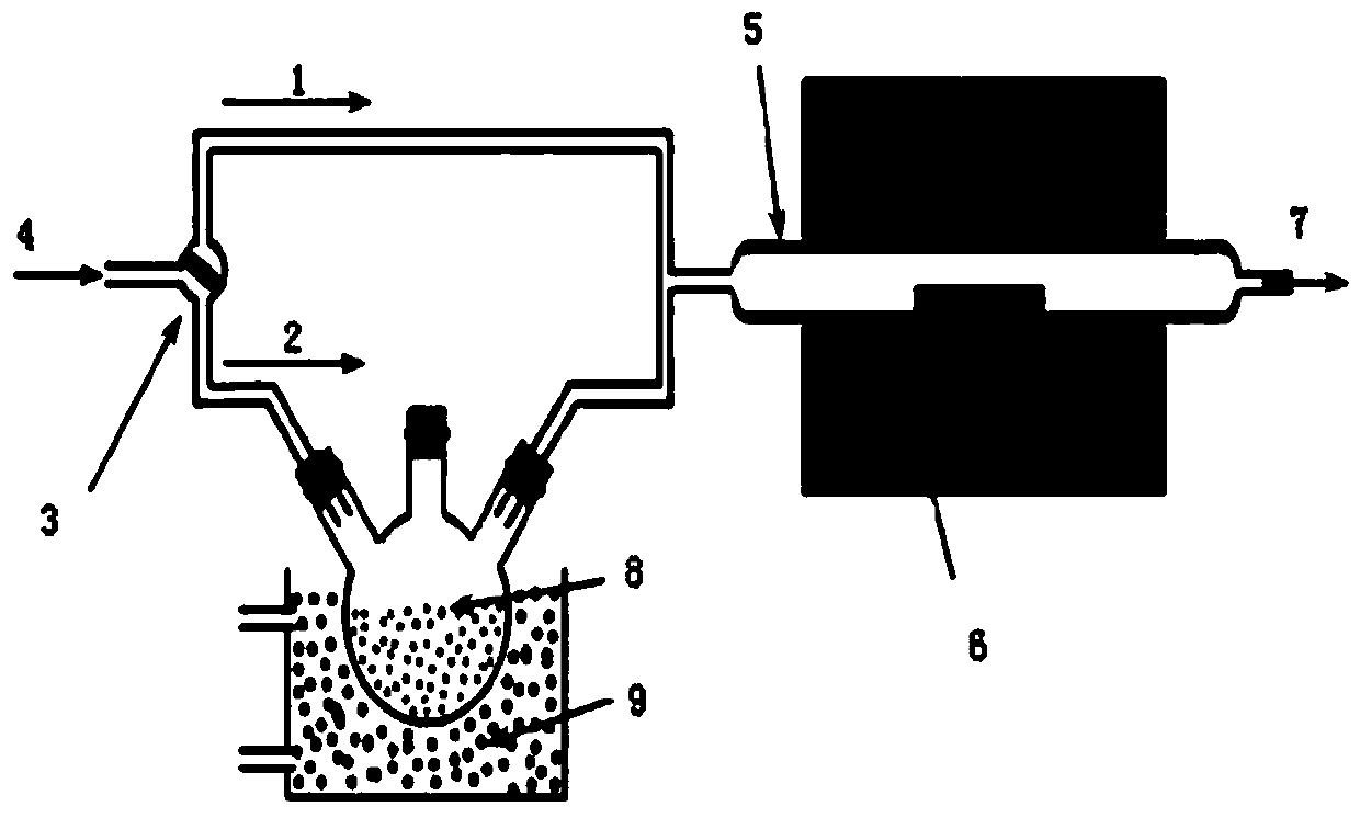
[0042] Put the Si substrate substrate into the reaction chamber of the chemical vapor deposition CVD system, and evacuate the reaction chamber to 10 -7 mbar level; at H 2 In the case of protection, the temperature of the reaction chamber is raised to the carbonization temperature of 900 ° C, and then the flow rate of 30 sccm is introduced into the reaction chamber. 3 h 8 , grow a layer of carbonized layer...

Embodiment 2

[0075] Step 1: same as step 1 of embodiment 1.

[0076] Step 2: growing a carbonized layer on the Si substrate, such as Figure 4 (b).

[0077]Put the Si substrate substrate into the reaction chamber of the chemical vapor deposition CVD system, and evacuate the reaction chamber to 10 -7 mbar level; at H 2 In the case of protection, the temperature of the reaction chamber is raised to the carbonization temperature of 1100 ° C, and then the flow rate of 30 sccm is introduced into the reaction chamber. 3 h 8 , grow a layer of carbonized layer on the Si substrate, the growth time is 6min.

[0078] Step 3: Epitaxial growth of 3C-SiC film, such as Figure 4 (c).

[0079] Raise the temperature of the reaction chamber rapidly to the growth temperature of 1300°C, and feed SiH with flow rates of 30sccm and 60sccm respectively. 4 and C 3 h 8 , carry out 3C-SiC film heteroepitaxial growth, the growth time is 45min; then in H 2 The temperature is gradually lowered to room tempera...

Embodiment 3

[0098] Step A: same as step 1 of embodiment 1.

[0099] Step B: Put the Si substrate substrate into the chemical vapor deposition CVD system reaction chamber, and vacuumize the reaction chamber to reach 10 -7 mbar level; at H 2 In the case of protection, the temperature of the reaction chamber is raised to 1200 ° C, and then the flow rate of 30 sccm is introduced into the reaction chamber. 3 h 8 , grow a layer of carbonized layer on the Si substrate, the growth time is 4min, the generated carbonized layer is as follows Figure 4 (b) shown.

[0100] Step C: Rapidly raise the temperature of the reaction chamber to 1350° C., and feed SiH at flow rates of 35 sccm and 70 sccm respectively 4 and C 3 h 8 , carry out 3C-SiC film heteroepitaxial growth, the growth time is 60min; then in H 2 Under protection, the temperature is gradually lowered to room temperature, and the growth of the 3C-SiC film is completed. The resulting 3C-SiC film is as follows: Figure 4 (c) shown.

[...


PUM

PropertyMeasurementUnit
lengthaaaaaaaaaa
thicknessaaaaaaaaaa

Abstract

The invention discloses a double-gate graphene transistor with a silicon substrate and an aluminium oxide gate dielectric, and a preparation method, which are mainly used for solving the problems of low channel carrier mobility and carrier scattering of a graphene transistor prepared by the prior art. The preparation method comprises the following realization steps of: depositing a layer of Al2O3 on an epitaxial 3C-SiC surface on a Si substrate, and photoetching a double-gate graph; placing the etched sample in a quartz tube, generating a carbon film by reacting Cl2 with SiC, then placing the carbon film sample in Ar gas and annealing to generate graphene; etching off Al2O3 at the both sides of the graphene sample and 60-400 nm away from a conductive channel to form a double-gate groove; finally depositing a metal layer on the graphene sample and etching to form transistor metal contact. The double-gate graphene transistor provided by the preparation method disclosed by the invention has the advantages of being high in carrier mobility, good in scattering effect suppression performance, and capable of regulating a channel carrier concentration, as well as can be used for producing a large-scale integrated circuit.

Description

technical field [0001] The invention belongs to the technical field of semiconductor devices, in particular to a double-gate graphene transistor, which can be used in large-scale integrated circuit production. technical background [0002] As people's demand for high-performance, high-reliability, and low-power equipment increases, more and more attention is paid to the characteristics of devices on integrated circuits. "Graphene", a material composed of a two-dimensional hexagonal carbon lattice, has been recognized by two scientists, Andre Jem and Kostya Novo, from the University of Manchester since 2004 due to its outstanding electrical structural properties. After Xiaoluofu was discovered, it was regarded as a candidate material for manufacturing high-performance devices. [0003] In 2005, Geim's research group and Kim's research group found that graphene has a thickness of about 10 cm at room temperature. 2 The high carrier mobility of / V s is about 10 times that of c...

Claims


Application Information

Patent Timeline
Patent Type & Authority Applications(China)
IPC IPC(8): H01L29/78H01L29/51H01L29/10H01L21/336
CPCH01L29/517H01L29/66045H01L29/78645
Inventor 郭辉赵亚秋张玉明黄海栗雷天民胡彦飞
Owner XIDIAN UNIV
Why Eureka
Try Eureka