Tungsten titanium alloy nanocrystalline gate-floating structure and preparation method thereof

A tungsten-titanium alloy and nanocrystalline technology, which is applied in the field of microelectronics to achieve good data retention characteristics, large physical thickness, and improve data retention characteristics and writing performance.

Inactive Publication Date: 2009-07-29
SEMICON MFG INT (SHANGHAI) CORP +1
View PDF6 Cites 2 Cited by
  • Summary
  • Abstract
  • Description
  • Claims
  • Application Information

AI Technical Summary

Problems solved by technology

Due to the limitation of the structure and material of the traditional floating gate structure memory cell, there is a serious contradiction between the requirement of fast write / erase operation and the requirement of long-term stable storage
And as the feature size shrinks, this contradiction becomes more significant

Method used


Image

  • Tungsten titanium alloy nanocrystalline gate-floating structure and preparation method thereof
  • Tungsten titanium alloy nanocrystalline gate-floating structure and preparation method thereof

Examples


Embodiment Construction

[0039] In order to make the object, technical solution and advantages of the present invention clearer, the implementation manner of the present invention will be further described in detail below in conjunction with the accompanying drawings.

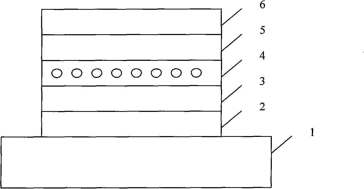
[0040] Such as figure 1 as shown, figure 1 Schematic diagram of the structure of the tungsten-titanium alloy nanocrystalline floating gate structure provided by the present invention.

[0041] The lowermost end of the structure is a silicon substrate 1, and the silicon substrate 1 is used to support the entire floating gate structure.

[0042] The silicon oxide layer 2 covered on the silicon substrate 1 has a thickness of 2nm to 4nm.

[0043] Cover the high dielectric constant film 3 on the silicon oxide layer 2, the composition of the high dielectric constant film can be HfO 2 Or HfAlO with a thickness of 4nm to 6nm.

[0044] The high dielectric constant film 3 is covered with a tungsten-titanium alloy nanocrystal charge storage l...


PUM

PropertyMeasurementUnit
thicknessaaaaaaaaaa
thicknessaaaaaaaaaa
diameteraaaaaaaaaa

Abstract

The invention discloses a tungsten-titanium alloy nanocrystalline floating grid structure used for a flash memory, pertaining to the technical field of micro-electronics. The structure comprises a silicon substrate as well as a silicon oxide layer, a high k (dielectric constant) thin film, a tungsten-titanium alloy nanocrystalline charge storage layer, a barrier layer and a grid material layer which are covered on the silicon oxide layer successively. The structure improves memory properties of a non-volatile memory unit of the floating grid structure, such as programming/erasing efficiency, programming/erasing (P/E) speed, effective charge memory power, data maintenance property and programming/erasing tolerance. The invention also discloses a method for manufacturing the tungsten-titanium alloy nanocrystalline floating grid structure. The method is simple and convenient and is compatible with the traditional CMOS silicon planar technology.

Description

technical field [0001] The invention relates to the technical field of microelectronics, in particular to a tungsten-titanium alloy nanocrystalline floating gate structure and a preparation method thereof. Background technique [0002] Floating gate non-volatile memory is a mainstream non-volatile memory that is widely used and generally recognized, and is widely used in electronic and computer equipment. Due to the limitation of the structure and material of the traditional floating gate structure memory cell, there is a serious contradiction between the requirement of fast write / erase operation and the requirement of long-term stable storage. And as the feature size shrinks, this contradiction becomes more significant. [0003] As the feature size advances to the nanometer level, improving the performance of reading, writing, erasing and maintaining stored data while reducing memory cells and increasing storage density has become a key issue facing the development of floa...

Claims


Application Information

Patent Timeline
Patent Type & Authority Applications(China)
IPC IPC(8): H01L29/49H01L21/28
Inventor 刘明杨仕谦王琴龙世兵
Owner SEMICON MFG INT (SHANGHAI) CORP
Why Eureka
Try Eureka