La-based medium material high-K metal gate structure based on Si substrate and preparation method thereof

A dielectric material and metal gate technology, which is applied in semiconductor/solid-state device manufacturing, semiconductor devices, electrical components, etc., can solve the problem of affecting the overall quality of the high-K metal gate structure, increasing the thickness of the equivalent oxide layer, and deteriorating the interface characteristics of the device, etc. problems, to achieve good conductivity, reduce power consumption, and increase the dielectric constant.

Inactive Publication Date: 2017-05-24
XIDIAN UNIV
View PDF4 Cites 0 Cited by
  • Summary
  • Abstract
  • Description
  • Claims
  • Application Information

AI Technical Summary

Problems solved by technology

However, due to the high diffusion coefficient of wafer Si in La-based high-k gate dielectric film, it is easy to form an interface layer with low dielectric constant, which will increase the equivalent oxide layer thickness and deteriorate the device interface characteristics.
[0004] On the other hand, in the traditional high-k metal gate structure, heavy metals are directly deposited on the high-k gate oxide layer as the gate electrode conductive layer, because the heavy metal ions will diffuse to the high-k gate oxide layer, and will be in the high-k gate oxide layer The introduction of impurities will seriously affect the overall quality of the high-K metal gate structure and increase the gate leakage current, thus affecting the reliability of the device

Method used


Image

  • La-based medium material high-K metal gate structure based on Si substrate and preparation method thereof
  • La-based medium material high-K metal gate structure based on Si substrate and preparation method thereof
  • La-based medium material high-K metal gate structure based on Si substrate and preparation method thereof

Examples


Embodiment 1

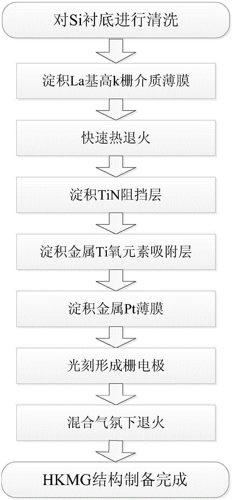
[0031] Embodiment 1: prepare La 2 o 3 High-k metal gate structure of high-k gate dielectric material.

[0032] Step 1, cleaning the silicon wafer.

[0033] 1a. Use NH in a ratio of 5:1:1 4 OH, H 2 o 2 and H 2 O equip SC-1 solution with HF and H at a ratio of 1:50 2 O equipped with HF solution;

[0034] 1b. Put the Si wafer in the SC-1 solution at a temperature of 75 ° C for 10 minutes, and rinse it with deionized water for 2 minutes to remove organic pollutants or attached particles on the Si wafer;

[0035] 1c. Place the Si wafer cleaned in the SC-1 solution in the HF solution for a second cleaning for 60 seconds, and rinse it with deionized water to remove the natural oxide layer SiO on the surface of the Si wafer 2 ;

[0036] 1d. Place the Si wafer after the second cleaning in deionized water and ultrasonically clean it for 5 minutes to remove the adsorbed particles on the surface, then rinse it with deionized water for 2 minutes, and dry it with 99.999% high-purity ...

Embodiment 2

[0063] Embodiment 2, preparation La 2 o 3 / Al 2 o 3 The stacked structure serves as a high-k metal gate structure with a high-k gate oxide layer.

[0064] Step 1, cleaning the silicon wafer.

[0065] The specific implementation of this step is the same as step 1 of Embodiment 1.

[0066] Step 2, put the cleaned Si wafer into the reaction chamber of the atomic layer deposition equipment, and use the atomic layer deposition method to deposit La on the dried Si wafer. 2 o 3 / Al 2 o 3 laminated film.

[0067] refer to Figure 4 and Figure 5 , the specific implementation of this step is as follows:

[0068] 2.1) In the ultra-clean room environment, put the pretreated and cleaned Si wafer into the reaction chamber of the atomic layer deposition equipment, then evacuate the chamber pressure to 15hPa, heat the temperature to 300°C, set the The 99.999% high-purity nitrogen flow used for washing is 120 sccm, and the deposition La 2 o 3 The number of cycles m and the depos...

Embodiment 3

[0097] Embodiment 3, preparation LaAlO 3 High-K metal gate structure of high-k gate oxide material.

[0098] Step A, cleaning the silicon wafer.

[0099] The specific implementation of this step is the same as step 1 of Embodiment 1.

[0100] Step B, put the cleaned Si wafer into the reaction chamber of the atomic layer deposition equipment, and use the atomic layer deposition method to deposit LaAlO on the dried Si wafer 3 film.

[0101] refer to Figure 6 , the specific implementation of this step is as follows:

[0102] B1. In the ultra-clean room environment, put the pretreated and cleaned Si wafer into the reaction chamber of the atomic layer deposition equipment, then evacuate the pressure of the chamber to 20hPa, heat the temperature to 310°C, and set the blower to The 99.999% high-purity nitrogen gas flow used for washing is 150 sccm, and the deposition La 2 o 3 The number of cycles m = 1, the deposition of Al 2 o 3 The number of cycles n=1;

[0103] B2. Depo...


PUM

PropertyMeasurementUnit
thicknessaaaaaaaaaa
thicknessaaaaaaaaaa
thicknessaaaaaaaaaa

Abstract

The invention discloses a La-based medium material high-K metal gate structure based on a Si substrate and a preparation method thereof, and mainly solves the problems that the gate oxide dielectric constant of the conventional high-K metal gate structure is low and gate metal is diffused to the gate oxide. The high-K metal gate structure comprises a La-based high-k gate medium film (1), a TiN barrier layer (2), a Ti oxygen adsorption layer (3) and a heavy metal Pt gate electrode (4) which are arranged on the Si substrate from the bottom to the top. A La2O3 or LaAlO3 or La2O3/Al2O3 laminated structure of which the thickness is 4-10nm is adopted for the La-based high-k gate medium film; the thickness of the TiN barrier layer is 2-3nm; the thickness of the Ti oxygen adsorption layer is 4-6nm; and the thickness of the heavy metal Pt gate electrode is 100-150nm. The gate oxide dielectric constant is high and the gate oxide/substrate interface property is great so that the structure can be used for manufacturing a high-dielectric-property metal oxide semiconductor field effect transistor.

Description

technical field [0001] The invention belongs to the technical field of semiconductor materials and devices, and in particular relates to a high-K metal gate structure and a preparation method, which can be used for manufacturing metal oxide semiconductor field effect transistors with high dielectric properties, and for the production and preparation of large-scale integrated circuits. Background technique [0002] With the continuous reduction of the integration level of integrated circuits, the size of the metal oxide semiconductor field effect transistor MOSFET is continuously reduced, and the corresponding gate oxide thickness is also continuously reduced. As of 2005, 65nm photolithography technology has become mature, and SiO2 as a gate dielectric film in high-performance field-effect transistor devices 2 The thickness of the layers has been reduced to around 1nm, that is, the spacing of only a few atomic layers. As the oxide thickness continues to decrease, the leakage...

Claims


Application Information

Patent Timeline
Patent Type & Authority Applications(China)
IPC IPC(8): H01L21/423H01L21/28
CPCH01L29/4232H01L21/28008H01L21/28194H01L29/42364
Inventor 刘红侠汪星赵璐冯兴尧王永特
Owner XIDIAN UNIV
Why Eureka
Try Eureka