A p-type insulated gate bipolar transistor structure

A technology of bipolar transistors and insulated gates, applied in semiconductor devices, electrical components, circuits, etc., can solve the problems of small β value of NPN tubes, restricting IGBT conduction current capability, etc., so as to improve the working current and vertical withstand voltage , the effect of increasing the magnification

Active Publication Date: 2016-08-17
SOUTHEAST UNIV
View PDF3 Cites 0 Cited by
  • Summary
  • Abstract
  • Description
  • Claims
  • Application Information

AI Technical Summary

Problems solved by technology

Due to the wide width of the P-epitaxial layer 4 (that is, the NPN tube base area) of the traditional structure IGBT, the β value of the NPN tube is very small, which restricts the conduction current capability of the IGBT

Method used


Image

  • A p-type insulated gate bipolar transistor structure
  • A p-type insulated gate bipolar transistor structure
  • A p-type insulated gate bipolar transistor structure

Examples


Embodiment Construction

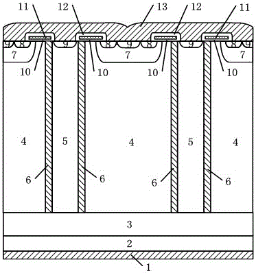
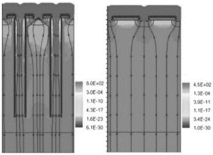
[0020] By adopting the N-type pillar narrow base transistor structure with a dielectric isolation layer of the present invention, the on-resistance of the device can be greatly reduced. With the development of semiconductor process technology, more power devices with low voltage drop, high current and high reliability can be produced by adopting the invention.

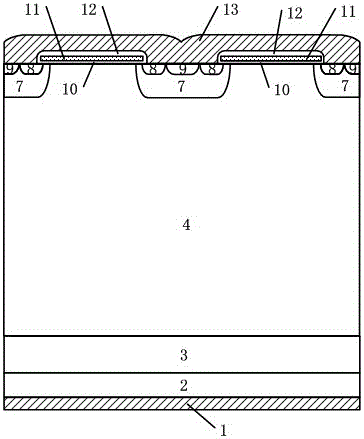
[0021] The P-type insulated gate bipolar transistor structure provided by the present invention includes an N-type doped silicon substrate that doubles as a collector region, and a collector metal is arranged under the N-type doped silicon substrate. A P-type doped silicon buffer layer is arranged above the silicon substrate, a P-type lightly doped silicon epitaxial layer is arranged above the P-type doped silicon buffer layer, and an N-type doped silicon epitaxial layer is arranged in the P-type lightly doped silicon epitaxial layer. The semiconductor region is provided with a P-type heavily doped semiconductor region...


PUM


Abstract

A p-type insulated gate bipolar transistor includes an N-type doped silicon substrate which is also used as a collector region; a collector metal is arranged beneath the N-type doped silicon substrate; a P-type doped silicon buffer layer and a P-type light doped silicon epitaxial layer are sequentially arranged above the N-type doped silicon substrate; the P-type light doped silicon epitaxial layer is internally provided with a N-type column; a P-type and an N-type heavily-doped semiconductor region are arranged in a N-type doped semiconductor region; the N-type column is internally provided with the N-type heavily-doped semiconductor region; a dielectric layer is arranged between the N-type column and the P-type light doped silicon epitaxial layer; a gate oxide layer and a polysilicon gate are sequentially arranged on the P-type light doped silicon epitaxial layer; the polysilicon gate begins above the dielectric layer and ends above the P-type heavily-doped semiconductor region which is adjacent to the dielectric layer; an oxide layer and an emitter metal are orderly arranged above the polysilicon gate; and the P-type and the N-type heavily-doped semiconductor region are electrically connected with the emitter metal.

Description

technical field [0001] The invention belongs to the technical field of power semiconductor devices, and relates to insulated gate bipolar transistors (IGBTs), more specifically, to a P-type insulated gate bipolar transistor structure with low on-resistance, high current capability, and high withstand voltage . Background technique [0002] At present, with the development of modernization and information age, semiconductor power devices play an increasingly important and irreplaceable role in power conversion, electric energy control and other fields. Nowadays, power devices are developing toward higher operating voltage, higher operating current, lower on-resistance, and higher reliability. The insulated gate bipolar transistor (IGBT) uses the conductance modulation effect to greatly reduce the conductance voltage drop. It can be used as an effective gate control switching device, catering to the development direction of power devices, and becoming a medium and high voltag...

Claims


Application Information

Patent Timeline
Patent Type & Authority Patents(China)
IPC IPC(8): H01L29/739H01L29/06
CPCH01L29/0603H01L29/7395
Inventor 孙伟锋戴伟楠杨卓孙华芳祝靖陆生礼时龙兴
Owner SOUTHEAST UNIV
Why Eureka
Try Eureka