A silicon carbide MOS gate-controlled thyristor
A thyristor, silicon carbide technology, applied in semiconductor devices, electrical components, circuits, etc., can solve the problems of large forward conduction resistance and low P-type cathode injection efficiency
- Summary
- Abstract
- Description
- Claims
- Application Information
AI Technical Summary
Problems solved by technology
Method used
Image
Examples
Embodiment Construction
[0018] The present invention is described in detail below in conjunction with accompanying drawing
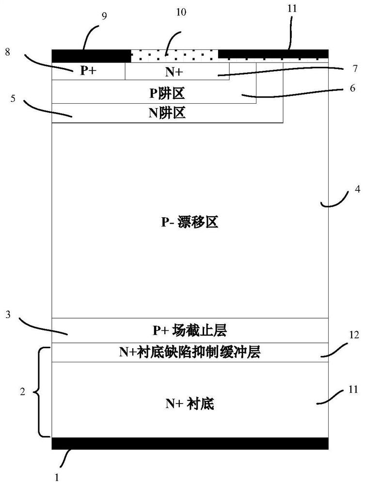
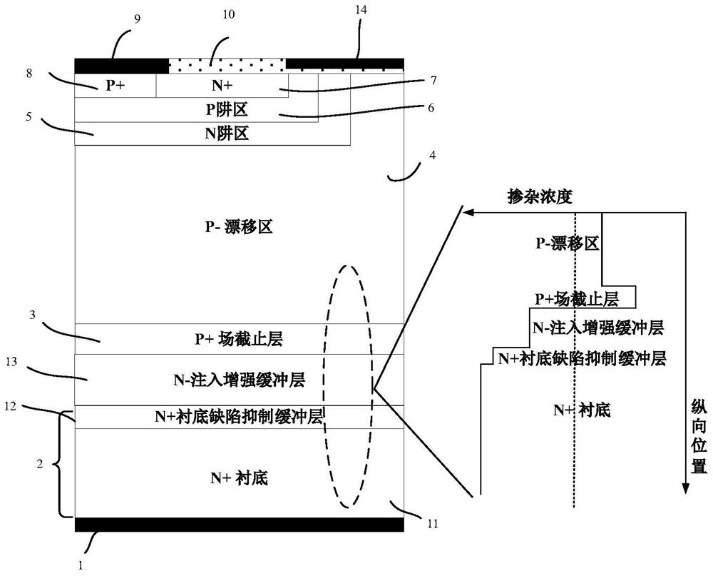
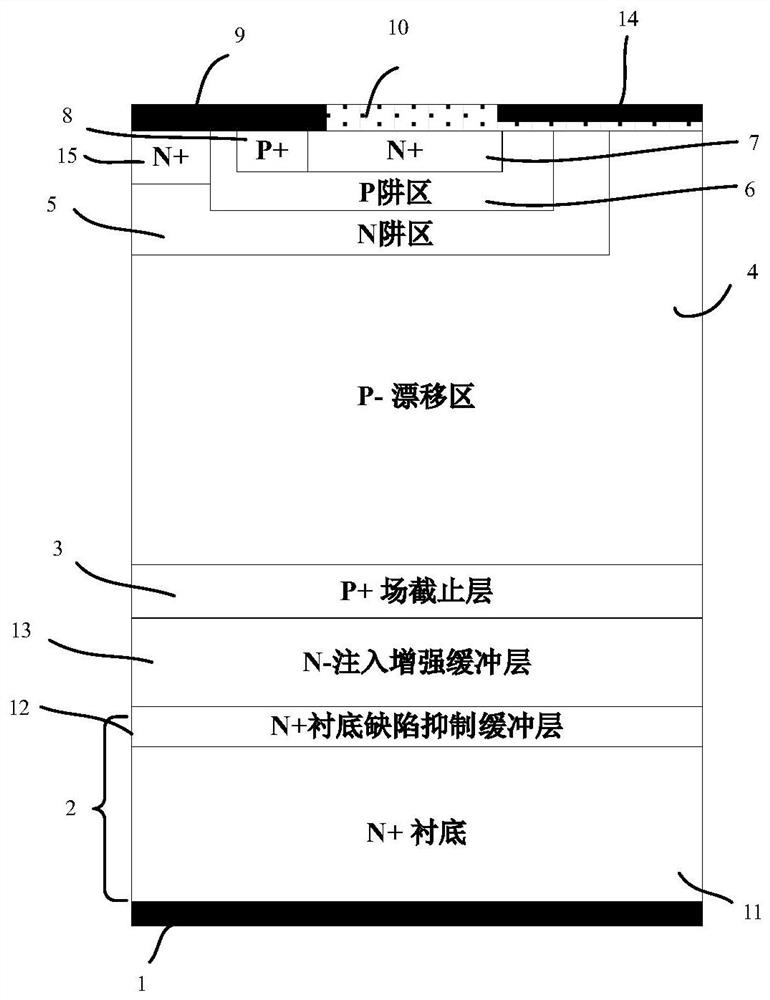
[0019] Such as figure 2 As shown, the silicon carbide MOS gate-controlled thyristor of the present invention has a cell structure including an anode structure, a gate structure, a drift region structure and a cathode structure; for a P-type silicon carbide MOS gate-controlled thyristor, its anode structure includes a P+ ohmic contact Region 8 and N+7 on its right side, and P+ ohmic contact region 8 and metal layer 9 on the upper surface of N+ region 7; the gate structure mainly includes N well region 5, P well region 6, and N well region The oxide layer 10 and the gate metal 14, the N+ region 7 and the P+ ohmic contact region 8 in the anode structure are within the P well region 6, the P well region 6 is inside the N well region 5, the gate metal 14 and the oxide layer 10 Covering the N+ region 7, the P well region 6 and the N well region 6; the drift region structure includes...
PUM
| Property | Measurement | Unit |
|---|---|---|
| thickness | aaaaa | aaaaa |
Abstract
Description
Claims
Application Information


