Anti-radiation common-island LPNP and SPNP layout structure
A technology of layout structure and radiation resistance, applied in the direction of electrical components, electric solid devices, circuits, etc., can solve the problems such as the decrease of the magnification of the SPNP tube, the decrease of the current collection capacity of the emission area, and the influence of the radiation resistance performance of the circuit, so as to save the layout. area, improve the anti-radiation performance, and stabilize the effect of the DC operating point
- Summary
- Abstract
- Description
- Claims
- Application Information
AI Technical Summary
Problems solved by technology
Method used
Image
Examples
Embodiment 1
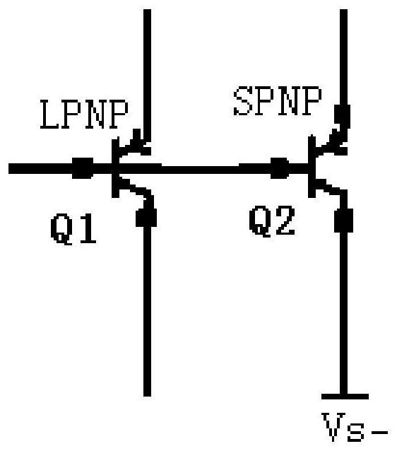
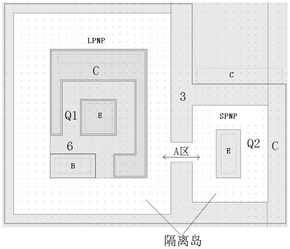
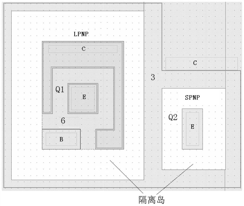
[0029] Such as image 3 and Figure 4 As shown, a radiation-resistant common-island LPNP and SPNP layout structure of the present invention includes a base 11 of LPNP, a collector 12 of LPNP, an emitter 13 of LPNP, an emitter 21 of SPNP, a base compound wall 3, Substrate 4 , epitaxial layer channel resistance 5 and buried layer 6 .
[0030] The surface of the substrate 4 is covered with an N-type epitaxial layer, and a buried layer 6 is arranged between the N-type epitaxial layer and the substrate 4; the base 11 of the LPNP and the collector of the LPNP are sequentially arranged on the N-type epitaxial layer 12. The emitter 13 of LPNP, the base compound wall 3 and the emitter E21 of SPNP; the base 11 of LPNP is connected to one end (point A) of the epitaxial channel resistance 5 through the epitaxial layer, and the other end (point A) of the epitaxial channel resistance 5 ( Point B), connect the base of SPNP; the base compound wall 3 separates the common island LPNP and SPNP...
Embodiment 2
[0035] The radiation-resistant common-island LPNP and SPNP layout structure in Embodiment 1 can improve the radiation resistance performance, but there is a risk of pinch-off of the base region of the SPNP tube. There is an epitaxial layer channel resistance Repi between the SPNP and LPNP bases. In actual work, when the potential of the epitaxial layer (the base of LPNP and SPNP) rises, the depletion layer 7 between the composite wall P+ and the epitaxial layer will widen, the resistance channel will be narrowed, and the resistance will increase. When the resistance channel is sandwiched When it is off, the SPNP base is open circuit, and the SPNP will not work normally.
[0036] Such as Figure 5 As shown, when the voltages of A and B (the bases of LPNP and SPNP) are close to the wall voltage Vs- of the isolation wall 8, the depletion layer 7 is relatively narrow, and there is an N-type epitaxial resistance channel between A and B. As A, As the B node voltage rises, the widt...
PUM
 Abstract
Description
Claims
Application Information


