Method for manufacturing display panel, display panel and display device

a technology of display panel and display panel, applied in the field of display technologies, can solve problems such as affecting the display

Active Publication Date: 2019-04-04
BOE TECH GRP CO LTD +1
View PDF3 Cites 2 Cited by
  • Summary
  • Abstract
  • Description
  • Claims
  • Application Information

AI Technical Summary

Benefits of technology

[0031]In an embodiment, the step of reducing the graphene oxide-polyacrylic acid solution comprises:
[0032]reducing graphene oxide in the graphene oxide-polyacrylic acid solution to graphene, and reducing polyacrylic acid in the graphene oxide-polyacrylic acid solution to polyimide, with a chemical reduction or a thermal reduction.

Problems solved by technology

On the other hand, when the assembled display panel is bent, the spacers are not fixed relative to the array substrate, which will affect the display effect.

Method used


Image

  • Method for manufacturing display panel, display panel and display device
  • Method for manufacturing display panel, display panel and display device

Examples


Embodiment Construction

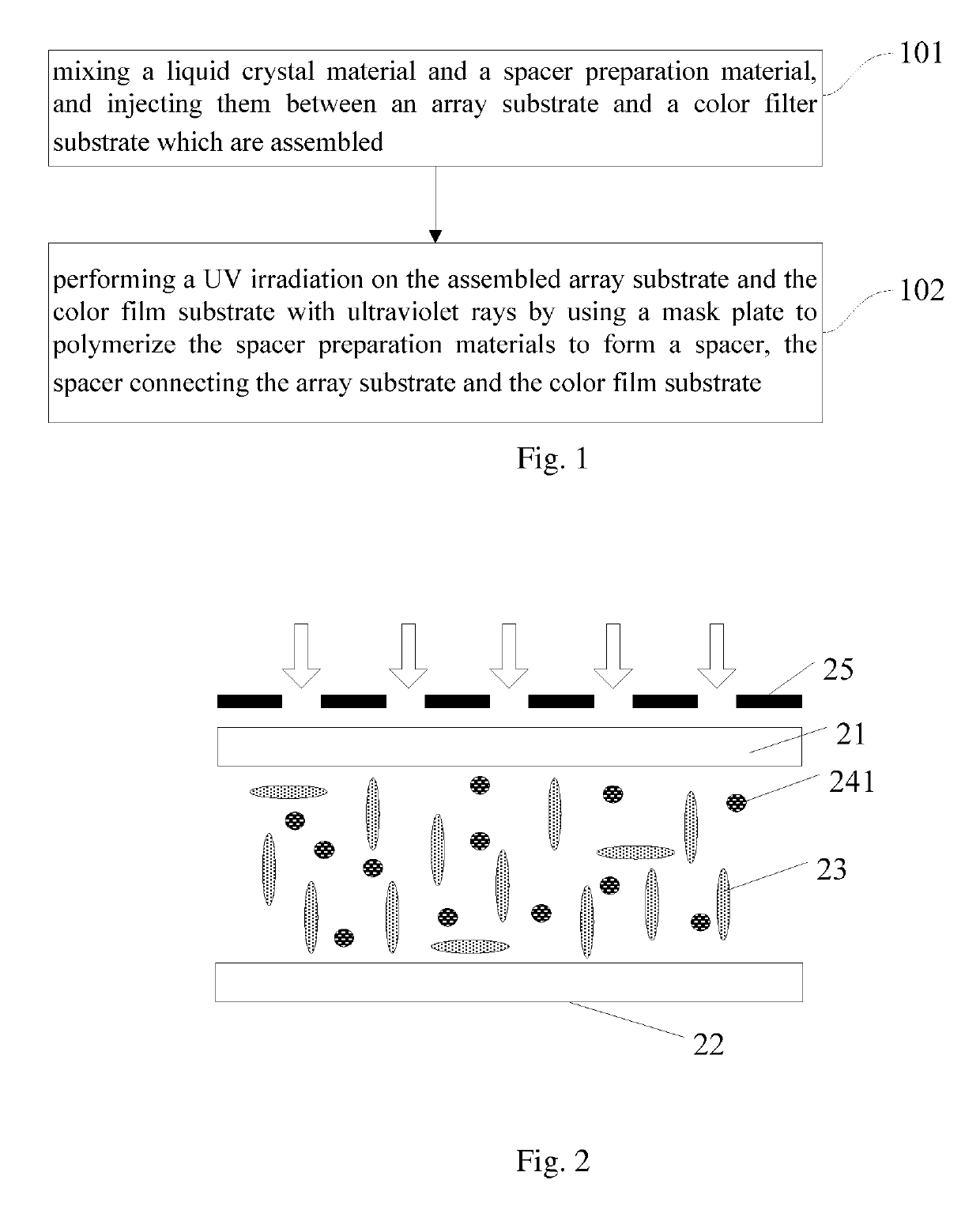
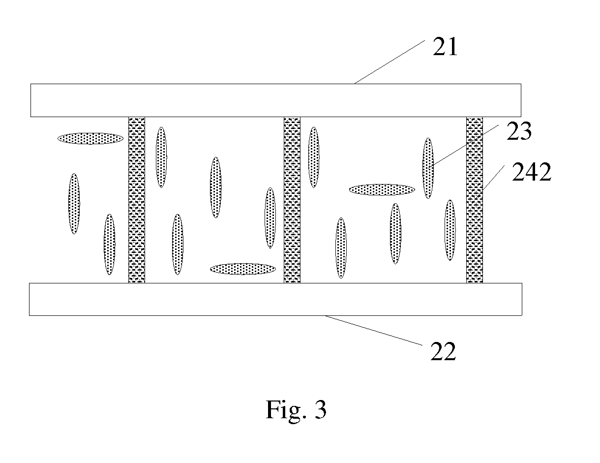
[0043]In order to make the above objects, features, and advantages of the present disclosure more comprehensible, the present disclosure will be further described in detail with reference to the accompanying drawings and specific embodiments. Referring to FIG. 1, a flowchart of a method for manufacturing a display panel according to an embodiment of the present disclosure is shown.

[0044]In step 101, mixing a liquid crystal material and a spacer preparation material, and injecting them between an array substrate and a color filter substrate which are aligned and assembled.

[0045]In the embodiment of the present disclosure, the liquid crystal material and the conductive spacer preparation material are mixed to obtain a mixture, the array substrate and the color filter substrate are aligned and assembled, and then the mixture is injected between the assembled array substrate and the color filter substrate.

[0046]The conductive spacer preparation material is a polymerizable monomer doped ...


PUM

PropertyMeasurementUnit
thicknessaaaaaaaaaa
coloraaaaaaaaaa
conductiveaaaaaaaaaa

Abstract

A method for manufacturing a display panel, a display panel and a display device are provided. The method for manufacturing a display panel includes: mixing a liquid crystal material and a spacer preparation material, and injecting them between an array substrate and a color filter substrate which are assembled; performing a UV irradiation on the assembled array substrate and the color film substrate with ultraviolet rays by using a mask plate to polymerize the spacer preparation material to form spacers, the spacers connecting the array substrate and the color film substrate.

Description

CROSS-REFERENCE TO RELATED APPLICATION[0001]This application claims the benefit of Chinese Patent Application No. 201710909879.5 filed on Sep. 29, 2017 in the State Intellectual Property Office of China, the whole disclosure of which is incorporated herein by reference.BACKGROUND OF THE INVENTIONField of the Invention[0002]The present disclosure relates to the field of display technologies, and in particular, to a method for manufacturing a display panel, a display panel, and a display device.Description of the Related Art[0003]In a manufacturing method of the related art, spacers thus formed may usually be fixed only to a color filter substrate. Then, in a process of aligning and assembling the color filter substrate and an array substrate, if the spacers are subjected to an external force, the spacers slide at corresponding positions on the array substrate. On the other hand, when the assembled display panel is bent, the spacers are not fixed relative to the array substrate, which...

Claims


Application Information

Patent Timeline
Patent Type & Authority Applications(United States)
IPC IPC(8): G02F1/1339G02F1/1337C09K19/56C01B32/198
CPCG02F1/13394G02F1/133723G02F1/133788C09K19/56C01B32/198G02F2001/13398G02F2202/16G02F2202/022G02F2001/133796G02F2202/36G02F1/13398G03F7/2002G03F7/027G02F1/133796
Inventor CAO, WEI
Owner BOE TECH GRP CO LTD
Why Eureka
Try Eureka