
Structure for radiofrequency applications

a radiofrequency application and structure technology, applied in the direction of basic electric elements, semiconductor devices, electrical equipment, etc., can solve the problems of reducing the density of the layer, the overall cost of the solution is too high, and the effect of reducing the effect of parasitic conduction and increasing the effect of resistivity of the substra

Active Publication Date: 2019-05-23
S O I TEC SILICON ON INSULATOR THECHNOLOGIES
View PDF4 Cites 1 Cited by
  • Summary
  • Abstract
  • Description
  • Claims
  • Application Information

AI Technical Summary

Benefits of technology

The patent text describes a way to prevent the movement of electrical charges in a semiconductor material, which can cause damage to RF devices. This is done by using a highly resistive material to insulate certain zones from each other. The result is an increased effective resistivity of the substrate, which reduces parasitic conduction and harmful effects on RF devices.

Problems solved by technology

For example, the antenna switches and power amplifiers manufactured on this type of substrate exhibit very good factors of merit but are mainly used for niche applications because of the too high overall cost of the solution.
Nevertheless, a poly-silicon trapping layer has the disadvantage of undergoing partial recrystallization during high temperature heat treatment steps, which contributes to reducing the density of traps in the layer.
The degradation of the RF device performance related to this decrease in the density of traps may be prohibitive for certain applications.
Moreover, these substrates struggle to ensure the stability of the RF performances over the entire range of operating temperatures, particularly above 100° C. Their resistivity falls considering the generation of thermal carriers in the support substrate and the coupling device / substrate becomes a major contributor to signal attenuation and distortion.
Other support substrates, such as aluminum nitride or silicon carbide, would meet the RF properties specifications but are not compatible with the standard semiconductor industry.
Nevertheless, the cost of these specific materials combined with that of the circuit transfer technologies is still too high for a mass adoption of these solutions.

Method used


Image

  • Structure for radiofrequency applications
  • Structure for radiofrequency applications
  • Structure for radiofrequency applications

Examples


Embodiment Construction

[0061]In the descriptive part, the same references in the figures may be used for elements of the same type. The figures are schematic representations which, for the sake of clarity, are not to scale. In particular, the thicknesses of the layers along the Z axis are not to scale with respect to the lateral dimensions along the X and Y axes, and the relative thicknesses of the layers between them are not necessarily respected in the figures.

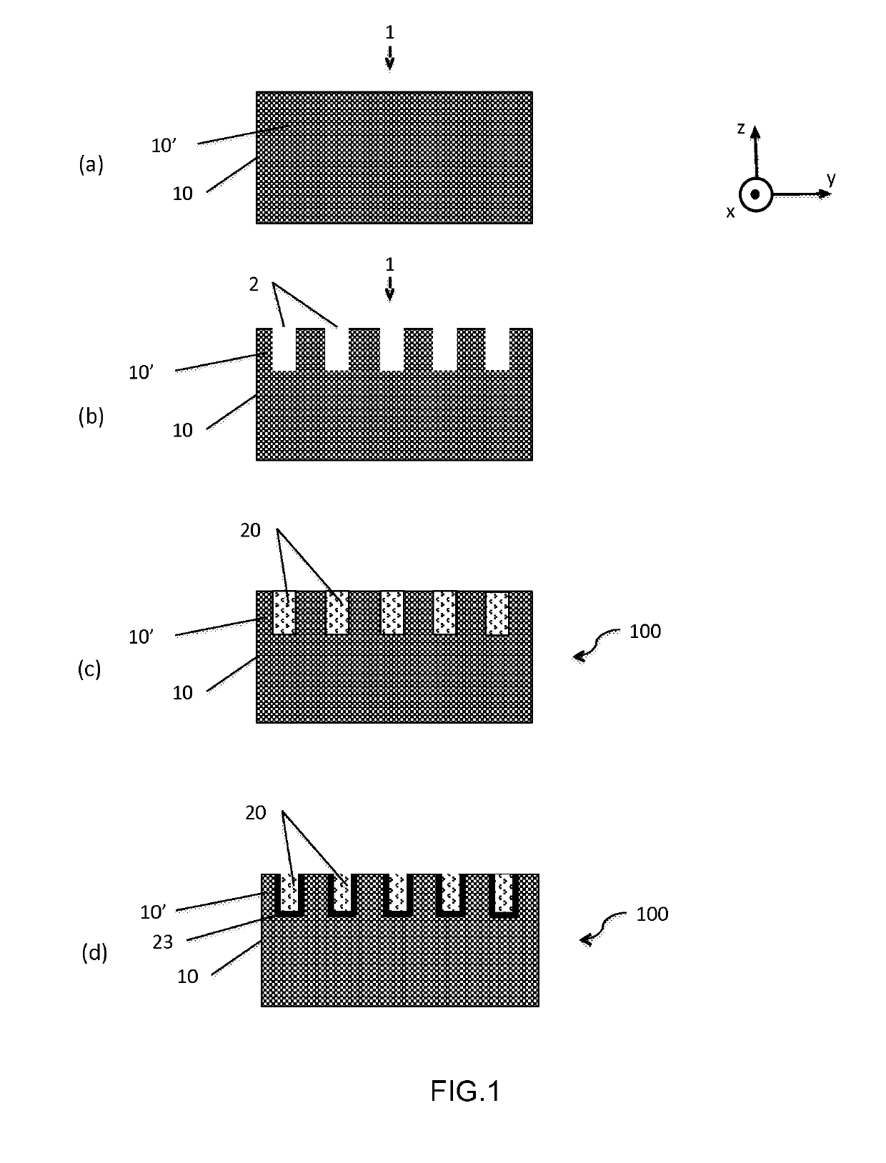
[0062]The disclosure relates to a method for producing a substrate suitable for microelectronic radiofrequency devices, shown in FIG. 1, Panels (a) through (c). The method includes providing a support substrate 10 with a first semiconductor material 10′ whose resistivity is greater than 500 ohms·cm (FIG. 1, Panel (a)). Advantageously, the resistivity of the first material will even be chosen to be greater than 1,000 ohms·cm, or even greater than 3,000 ohms·cm. As illustration, the first semiconductor material 10′ may be monocrystalline silicon.

[00...


PUM


Abstract

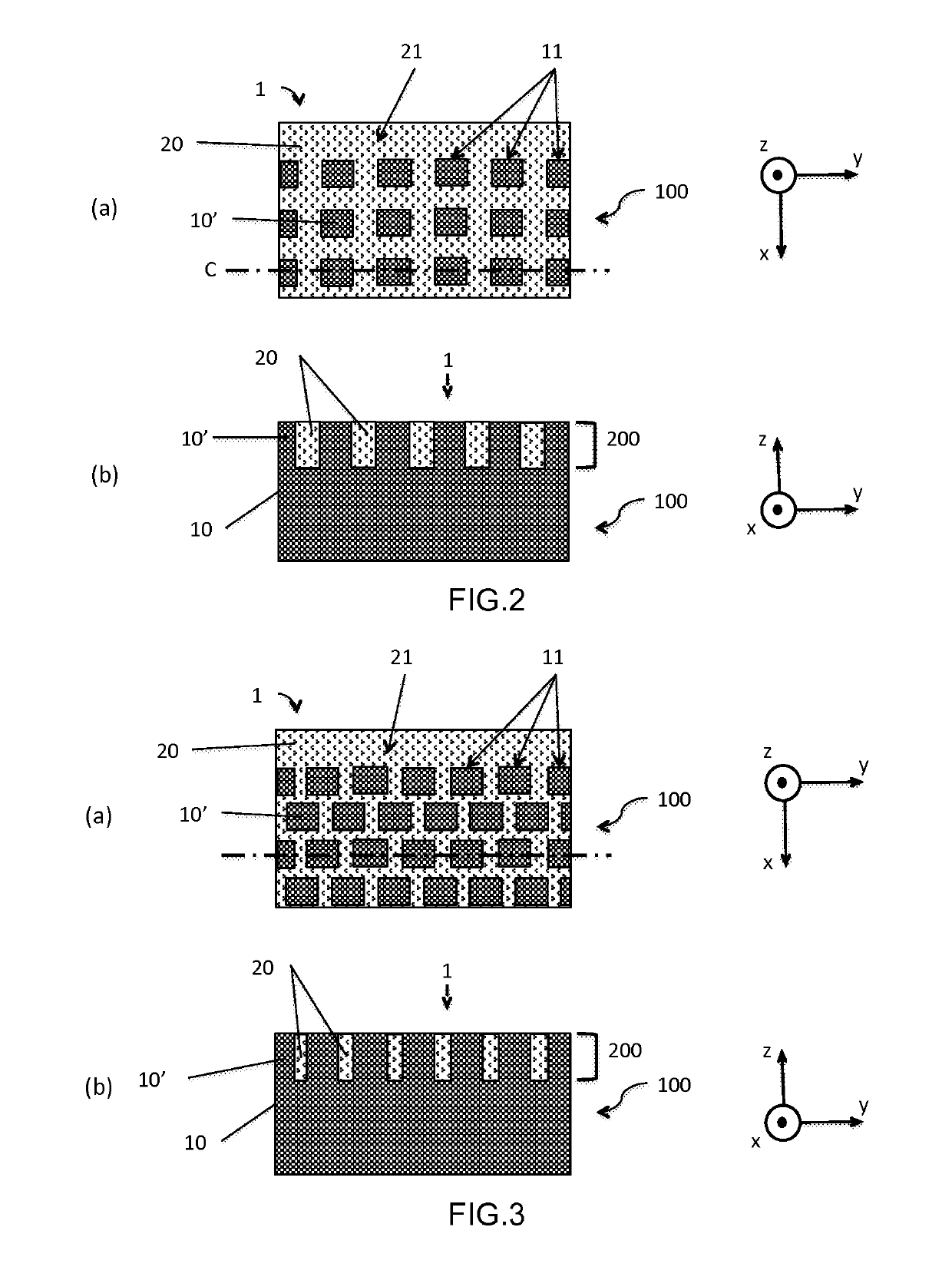
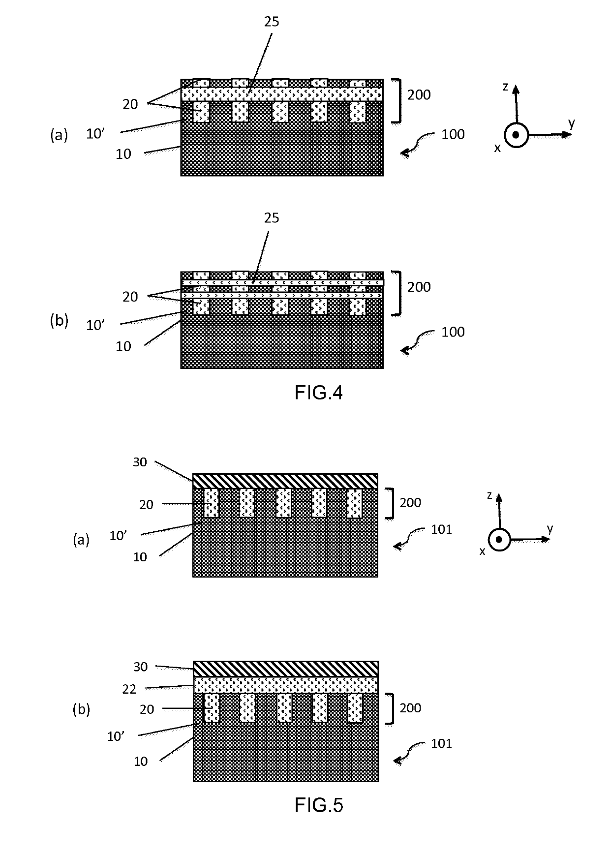
A substrate for microelectronic radiofrequency devices includes a carrier substrate made of a first semiconductor material having a resistivity higher than 500 ohms·cm; a plurality of trenches in the carrier substrate, which trenches are filled with a second material, and defining on a first side of the carrier substrate a plurality of first zones made of a first material and at least one second zone made of a second material. The second material has a resistivity higher than 10 kohms·cm, and the first zones have a maximum dimension smaller than 10 microns and are insulated from one another by the second zone.

Description

CROSS-REFERENCE TO RELATED APPLICATIONS[0001]This application is a national phase entry under 35 U.S.C. § 371 of International Patent Application PCT / FR2017 / 051418, filed Jun. 6, 2017, designating the United States of America and published as International Patent Publication WO 2017 / 212160 A1 on Dec. 14, 2017, which claims the benefit under Article 8 of the Patent Cooperation Treaty to French Patent Application Serial No. 1655266, filed Jun. 8, 2016.TECHNICAL FIELD[0002]The present disclosure relates to the field of integrated radio frequency devices.BACKGROUND[0003]For most applications involving the transmission or reception of radio frequency signals (10 MHz to 100 GHz), the devices require a substrate that increasingly fulfills demanding specifications, particularly driven by the changing standards of mobile telephony (2G, 3G, LTE, LTE Advanced, LTE Advanced PRO, 5G . . . ). The properties of substrate materials must specifically ensure:[0004]Low insertion losses (low signal att...

Claims


Application Information

Patent Timeline
Patent Type & Authority Applications(United States)
IPC IPC(8): H01L21/762H01L21/84H01L27/12H01L29/06
CPCH01L21/76283H01L21/84H01L21/76224H01L27/1203H01L29/0649H01L21/02002H01L21/76264H01L27/1218H01L29/78603H01L21/76254
Inventor DESBONNETS, ERICRADU, IONUTKONONCHUK, OLEGRASKIN, JEAN-PIERRE
Owner S O I TEC SILICON ON INSULATOR THECHNOLOGIES
Learn More