
Flexible substrate and manufacturing method thereof

a flexible substrate and manufacturing method technology, applied in the field of display technology, can solve the problems of low manufacturing yield, loss of light, and reducing the reflection rate of alignment marks, so as to reduce the thickness of edges, reduce the coverage area of organic materials, and improve the reflection rate at alignment marks

Active Publication Date: 2019-05-23
WUHAN CHINA STAR OPTOELECTRONICS TECH CO LTD
View PDF5 Cites 0 Cited by
  • Summary
  • Abstract
  • Description
  • Claims
  • Application Information

AI Technical Summary

Benefits of technology

This patent describes a flexible substrate that improves alignment accuracy, increases light transmission, reduces warping, and prevents etching residue at the edges. The substrate is made by coating a carrying plate with two layers of organic material, where the second layer has a larger coverage area and encloses the first layer to reduce warping and etching residue. An alignment mark is formed on the second layer for better alignment accuracy. The manufacturing method provides a flexible substrate with high alignment accuracy and product yield, increased light transmission, better successful alignment, reduced warming, and less etching residue.

Problems solved by technology

However, the larger the area that the organic material substrate covers the carrying glass plate, the greater the warpage that organic material substrate may generate in an array process and the lower the manufacturing yield.
Further, since the flexible organic material substrate that is used in the contemporary LTPS flexible OLED display device is often a colorful temperature-resistant organic material, in alignment for vapor deposition, alignment light gets incident from a back side of the flexible organic material substrate, transmitting through the colorful flexible organic material substrate may lead to loss of light, so as to reduce the reflection rate of the alignment mark and thus affecting the rate of successful alignment.

Method used

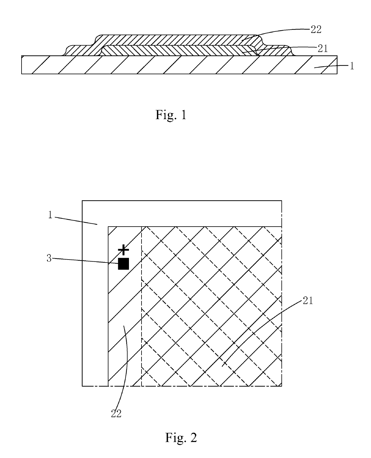
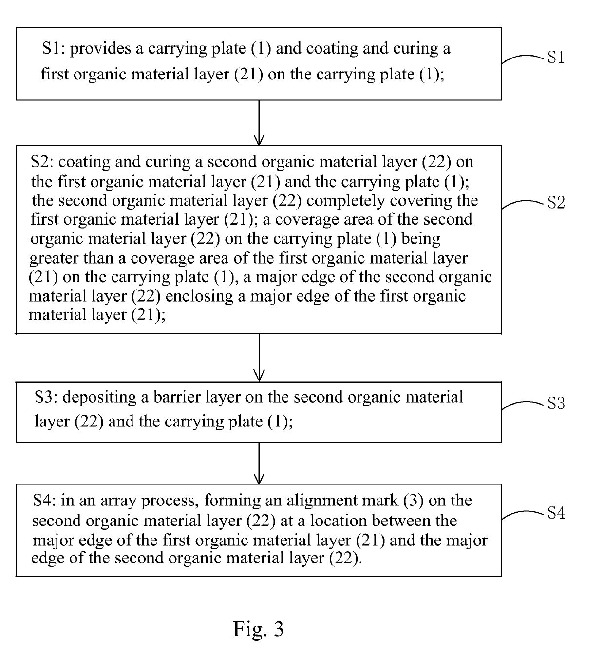

Image

  • Flexible substrate and manufacturing method thereof
  • Flexible substrate and manufacturing method thereof

Examples


Embodiment Construction

[0032]To further expound the technical solution adopted in the present invention and the advantages thereof, a detailed description will be given with reference to the preferred embodiments of the present invention and the drawings thereof

[0033]Referring simultaneously to FIGS. 1 and 2, firstly, the present invention provides a flexible substrate, which comprises a first organic material layer 21 laid on a carrying plate 1 and a second organic material layer 22 completely covering the first organic material layer 21. A coverage area of the second organic material layer 22 on the carrying plate 1 is greater than a coverage area of the first organic material layer 21 on the carrying plate 1 and a major, long edge of the second organic material layer 22 surrounds a major, long edge of the first organic material layer 21.

[0034]Specifically, the carrying plate 1 is preferably a glass plate; and the first organic material layer 21 and the second organic material layer 22 are each formed ...


PUM


Abstract

The present invention provides a flexible substrate and a manufacturing method thereof. The flexible substrate is divided into a first organic material layer (21) and a second organic material layer (22). A coverage area of the second organic material layer (22) on a carrying plate (1) is greater than a coverage area of the first organic material layer (21) on the carrying plate (1) and a major, long edge of the second organic material layer (22) encloses a major, long edge of the first organic material layer (21) so as to help reduce the thickness of an edge of the flexible substrate and prevent etching residue at an edge, reduce the coverage area of the organic materials on the carrying plate, and reduce warpage of the flexible substrate. Further, an alignment mark (3) is formed on the second organic material layer (22) at a location between the major, long edge of the first organic material layer (21) and the major, long edge of the second organic material layer (22) to ensure alignment accuracy in subsequent processes, such as vapor deposition. Further, since there is only one layer of organic material at the site of alignment mark (3), light transmission rate is increased and the rate of successful alignment is enhanced.

Description

BACKGROUND OF THE INVENTION1. Field of the Invention[0001]The present invention relates to the field of display technology, and more particular to a flexible substrate and a manufacturing method thereof.2. The Related Arts[0002]Organic light emitting display (OLED) is a display technology of prosperous future of development for it has excellent displaying performance and also shows various advantages including being self-luminous, simple structure, being ultra light and thin, fast response speed, wide view angle, low power consumption and realization of flexible displaying and is thus regarded as a “dream display”, attracting attention of major display manufacturers, making it the main force of the third generation displays in the field of display technology.[0003]A flexible OLED display device requires formation of an arrayed arrangement of pixel structures on a substrate and each pixel structure generally comprises components including a thin-film transistor (TFT) and a capacitor....

Claims


Application Information

Patent Timeline
Patent Type & Authority Applications(United States)
IPC IPC(8): H01L51/00H01L51/56H10K99/00
CPCH01L51/0097H01L51/56H10K59/12H10K77/111H10K71/00Y02E10/549Y02P70/50
Inventor QIN, FANG
Owner WUHAN CHINA STAR OPTOELECTRONICS TECH CO LTD
Learn More