Micro light-emitting diode display device and manufacturing method thereof

a light-emitting diode and display device technology, applied in the field of display technology, can solve the problems of large technical difficulty and long transfer process, and achieve the effects of reducing technical difficulty, simplifying manufacturing process, and reducing time of transferring light-emitting diodes

Active Publication Date: 2019-05-30
WUHAN CHINA STAR OPTOELECTRONICS TECH CO LTD
View PDF1 Cites 3 Cited by
  • Summary
  • Abstract
  • Description
  • Claims
  • Application Information

AI Technical Summary

Benefits of technology

[0006]In view of the shortcomings of conventional technology, the present invention provides a micro light-emitting diode display device and a method of fabricating the same that reduces the number of transfer times for the LED and reduces the difficulty of the micro LED transfer technology.
[0024]The micro light-emitting diodes of the present invention all emit blue light. By means of transferring the micro LEDs to the substrate at one time, and making it to excite the yellow phosphor layer meanwhile cooperate with the color filter layer in a light-emitting direction, a color display purpose could be achieved, which reduces the times of transferring the light-emitting diodes, simplifies the manufacturing process, and reduces technical difficulty for transferring micro LED.

Problems solved by technology

Since such transfer involves a precise transfer for a large number of micro LED and a transfer of a large number of times, the transfer process takes a long time and its technical difficulty is quite large.

Method used


Image

  • Micro light-emitting diode display device and manufacturing method thereof
  • Micro light-emitting diode display device and manufacturing method thereof

Examples


Embodiment Construction

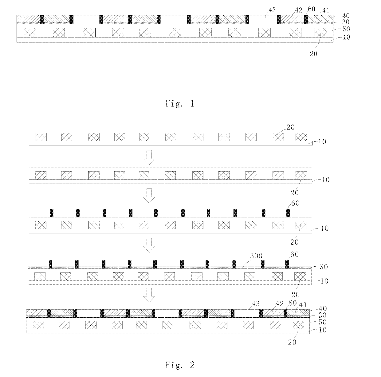
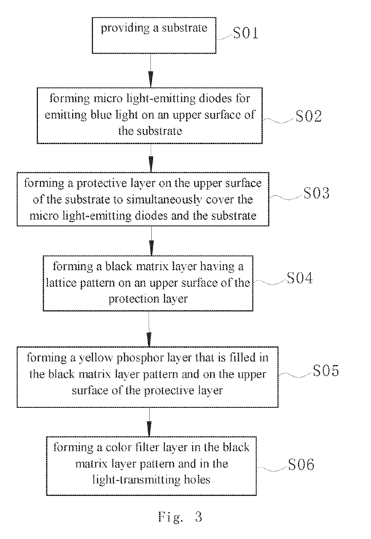
[0028]The specific structural and functional details disclosed herein are only representative and are intended for describing exemplary embodiments of the disclosure. However, the disclosure can be embodied in many forms of substitution, and should not be interpreted as merely limited to the embodiments described herein.

[0029]In the description of the disclosure, terms such as “center”, “transverse”, “above”, “below”, “left”, “right”, “vertical”, “horizontal”, “top”, “bottom”, “inside”, “outside”, etc. for indicating orientations or positional relationships refer to orientations or positional relationships as shown in the drawings; the terms are for the purpose of illustrating the disclosure and simplifying the description rather than indicating or implying the device or element must have a certain orientation and be structured or operated by the certain orientation, and therefore cannot be regarded as limitation with respect to the disclosure. Moreover, terms such as “first” and “s...


PUM

PropertyMeasurementUnit
light-transmitting areaaaaaaaaaaa
colorless transparentaaaaaaaaaa
lattice patternaaaaaaaaaa

Abstract

The present invention discloses a micro light-emitting diode display device comprising a substrate, micro light-emitting diodes arrayed on an upper surface of a substrate for emitting blue light, a yellow phosphor layer disposed on a light-emitting side of the micro light-emitting diodes, and a color filter layer disposed on a light-emitting side of the yellow phosphor layer. The color filter layer comprises a red filter area, a green filter area, and a light-transmitting area. The yellow phosphor layer is provided with light-transmitting holes opened to its surface at intervals, and the light-transmitting holes are directly opposite to the light-transmitting area. The present invention further provides a method of manufacturing a micro light emitting diode display device. A color display purpose is achieved, which reduces the times of transferring the light-emitting diodes, simplifies the manufacturing process, and reduces technical difficulty for transferring micro LED.

Description

RELATED APPLICATIONS[0001]The present application is a National Phase of International Application Number PCT / CN2017 / 114046, filed Nov. 30, 2017, and claims the priority of China Application 201711206341.4, filed Nov. 27, 2017.BACKGROUND OF THE INVENTION1. Field of the Invention[0002]The present invention relates to a field of display technology, and in particular, to a micro light-emitting diode display device and a manufacturing method thereof.2. The Related Arts[0003]Micro LED (micro-LED) technology, i.e., LED miniaturization matrix technology, refers to a high-density small-size LED arrays integrated on a single chip. Each pixel in the LED display panel can be addressed and driven individually. The micro LED display panel can be seen as a miniature version of an outdoor LED display panel, which reduces the pixel distance from a millimeter-level down to a micron-level.[0004]Micro LED has many advantages. It has the advantages of high efficiency, high brightness, high reliability ...

Claims


Application Information

Patent Timeline
Patent Type & Authority Applications(United States)
IPC IPC(8): H01L27/15H01L25/075G02B5/20G03F7/00G09G3/32G09G3/20
CPCH01L27/156H01L25/0753G09G3/2003G03F7/0007G09G3/32G02B5/201G09F9/33H01L25/167H01L33/44H01L33/505H01L33/507H01L2933/0025H01L2933/0041H01L2933/005G02B5/003
Inventor XU, HAILESHEN, SHUNJIESONG, JIANGJIANGZHAO, FENLI
Owner WUHAN CHINA STAR OPTOELECTRONICS TECH CO LTD
Why Eureka
Try Eureka