

Dynamic random access memory device
a random access and memory device technology, applied in the field of dynamic random access memory devices, can solve problems such as operation failures, and achieve the effect of reducing failures caused during operation
- Summary
- Abstract
- Description
- Claims
- Application Information
AI Technical Summary
Benefits of technology
Problems solved by technology
Method used
Image

Examples
Embodiment Construction
[0019]Hereinafter, dynamic random access memory (DRAM) devices according to example embodiments of the present inventive concept will be described with reference to the accompanying drawings.
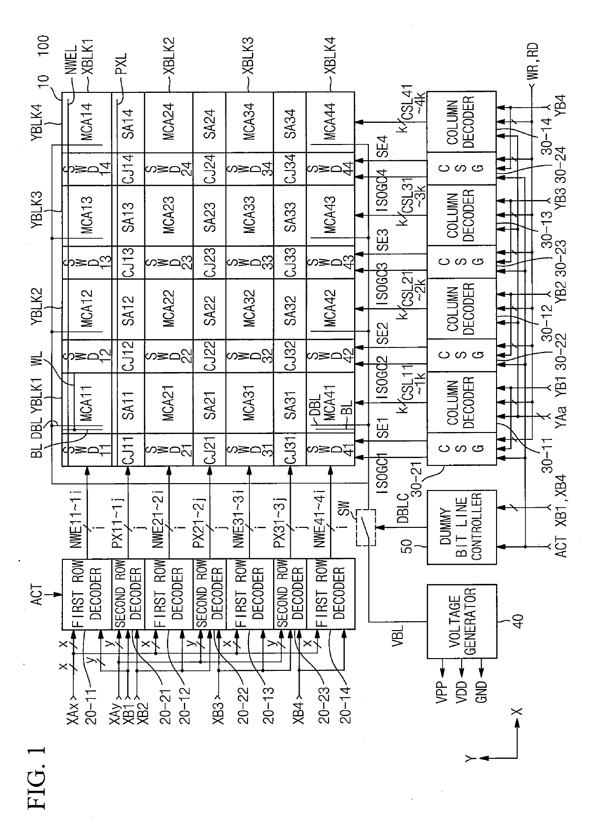
[0020]FIG. 1 is a diagram that illustrates an arrangement and a configuration of a DRAM device according to an example embodiment of the present inventive concept.
[0021]Referring to FIG. 1, a DRAM device 100 may include a memory cell array 10, first row decoders 20-11 to 20-14, second row decoders 20-21 to 20-23, column decoders 30-11 to 30-14, control signal generators (CSG) 30-21 to 30-24, a voltage generator 40, a dummy bit line controller 50, and a switch SW.
[0022]The memory cell array 10 may include four X memory cell array blocks XBLK1 to XBLK4 arranged in a bit line direction Y. The four X memory cell array blocks XBLK1, XBLK2, XBLK3, and XBLK4 may include four sub memory cell array blocks MCA11 to MCA14, MCA21 to MCA24, MCA31 to MCA34, and MCA41 to MCA44, respectively. The memory cell ar...
PUM
 Abstract
Description
Claims
Application Information