Thin film transistor substrate, liquid crystal display device including same, and method for producing thin film transistor substrate

Inactive Publication Date: 2019-06-27
SHARP KK
View PDF7 Cites 1 Cited by
  • Summary
  • Abstract
  • Description
  • Claims
  • Application Information

AI Technical Summary

Benefits of technology

[0021]The present invention can provide a thin film transistor substrate capable of stabilizing TFT characteristics and a method for produc

Problems solved by technology

Specifically, the threshold value may greatly shift to the negative side, or the oxide semiconductor layer may become conductive and thereby cause leakage current between the source electrode and the drain electrode.
The same troubles can occur also when a protective film (e.g.

Method used


Image

  • Thin film transistor substrate, liquid crystal display device including same, and method for producing thin film transistor substrate
  • Thin film transistor substrate, liquid crystal display device including same, and method for producing thin film transistor substrate
  • Thin film transistor substrate, liquid crystal display device including same, and method for producing thin film transistor substrate

Examples


Example

Embodiment 1

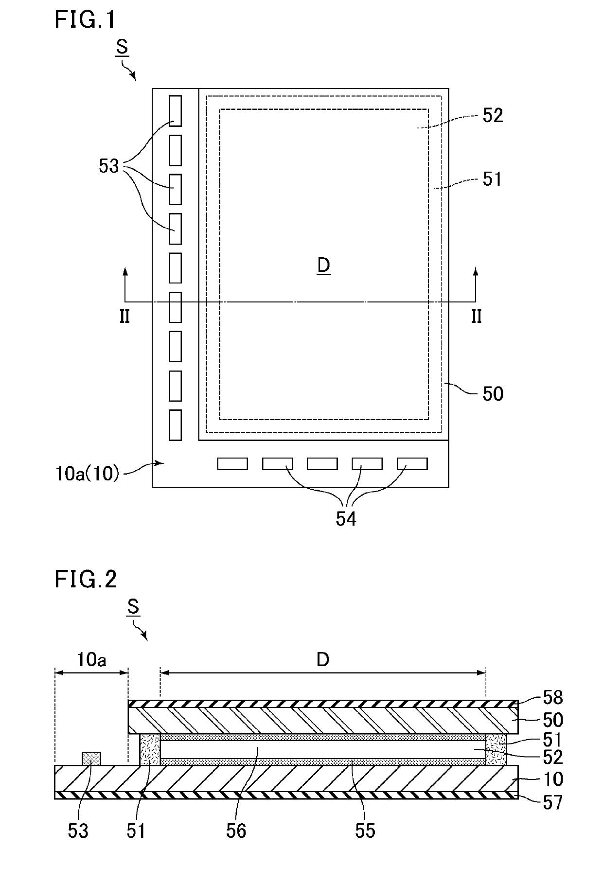
[0050]FIG. 1 is a schematic plan view of a liquid crystal display device S according to the present embodiment. FIG. 2 is a cross-sectional view illustrating a cross-sectional structure along the II-II line in FIG. 1. In FIG. 1, a polarizing plate 58 shown in FIG. 2 is omitted.

Structure of Liquid Crystal Display Device S

[0051]The liquid crystal display device S includes a TFT substrate 10 and a counter substrate 50 facing each other, a frame-shaped seal 51 bonding the peripheries of the TFT substrate 10 and the counter substrate 50, and a liquid crystal layer 52 sealed inside the seal 51 between the TFT substrate 10 and the counter substrate 50.

[0052]The liquid crystal display device S is a transmissive liquid crystal display device. The liquid crystal display device S has a display area D for image display in the region where the TFT substrate 10 and the counter substrate 50 overlap inside the seal 51, that is, the region where the liquid crystal layer 52 is formed. Out...

Example

Embodiment 2

[0105]The present embodiment mainly describes the characteristic features of the present embodiment, and omits the descriptions of the same features as those of Embodiment 1. In the present embodiment and Embodiment 1, members that exhibit the same or similar functions are donated by the same reference signs and the description of the members are omitted in the present embodiment. The present embodiment is substantially the same as Embodiment 1 except that the TFTs are etch stopper-type TFTs as described below.

Structure of TFT Substrate 10

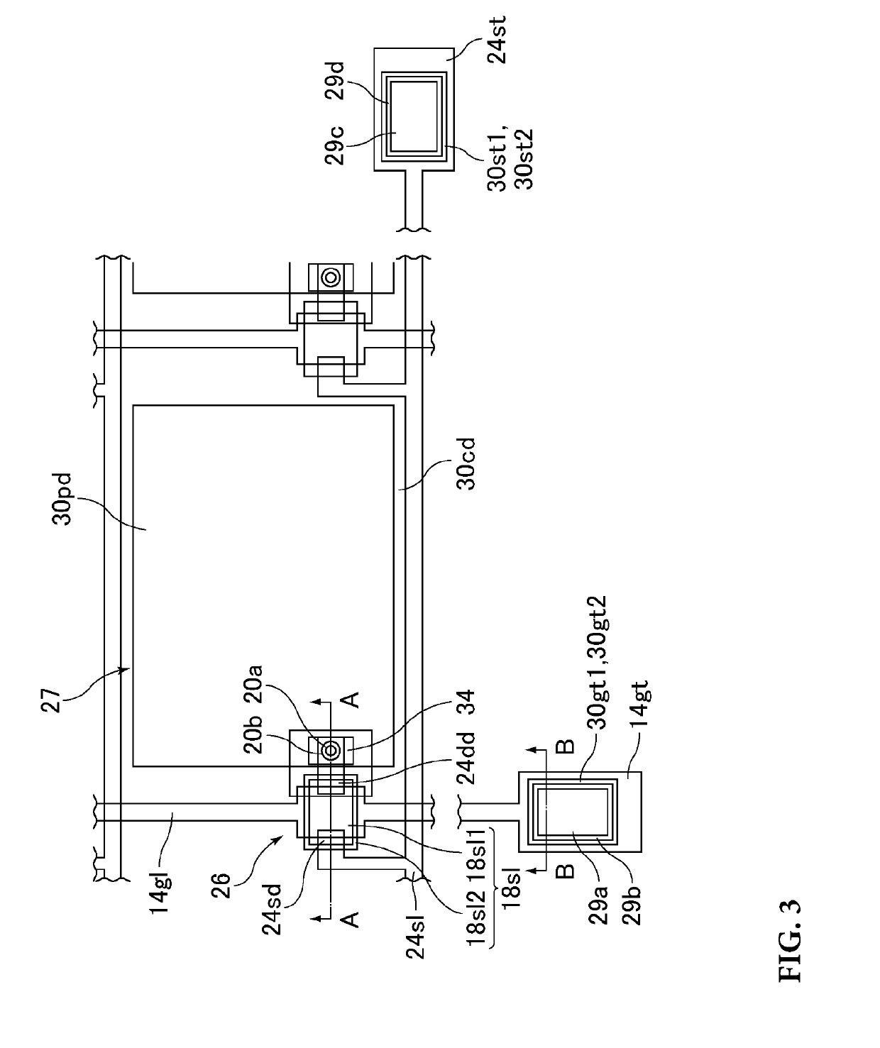
[0106]FIG. 15 and FIG. 16 are schematic views illustrating the TFT substrate 10 according to the present embodiment. FIG. 15 is a schematic plan view illustrating one pixel and the terminal of each line. FIG. 16 includes cross-sectional views illustrating, from left to right in the figure, cross-sectional structures along the A-A line and the B-B line in FIG. 15.

[0107]In the present embodiment, as shown in FIG. 15, the TFT substrate 10 ...

Example

Embodiment 3

[0120]The present embodiment mainly describes the characteristic features of the present embodiment, and omits the descriptions of the same features as those of Embodiments 1 and 2. In the present embodiment and Embodiments 1 and 2, members that exhibit the same or similar functions are donated by the same reference signs and the description of the members are omitted in the present embodiment. The present embodiment is substantially the same as Embodiment 1 except that the oxide semiconductor layer is arranged inside the gate electrode.

Structure of TFT Substrate 10

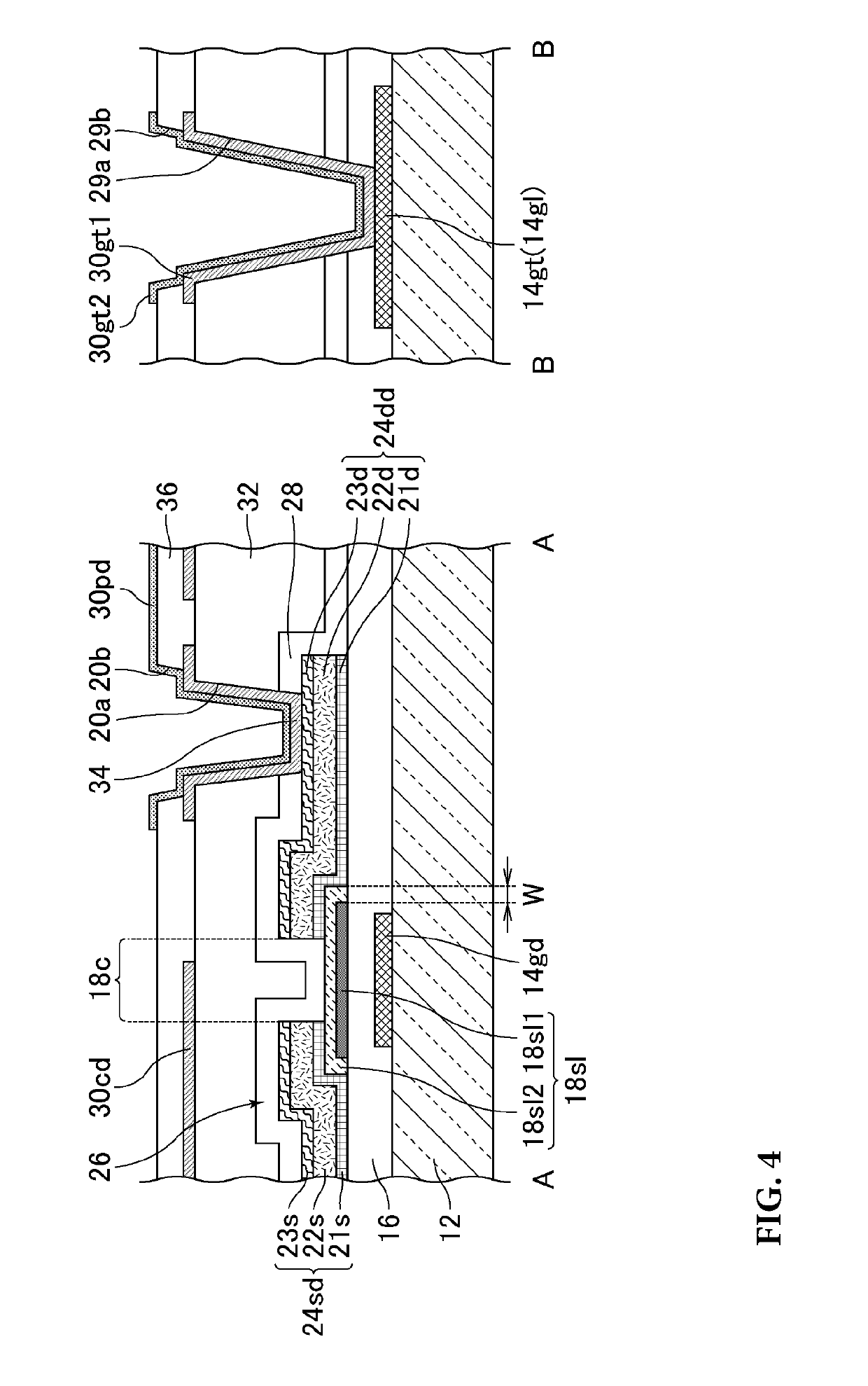
[0121]FIG. 19 and FIG. 20 are schematic views illustrating the TFT substrate 10 according to the present embodiment.

[0122]FIG. 19 is a schematic plan view illustrating one pixel and the terminal of each line. FIG. 20 includes cross-sectional views illustrating, from left to right in the figure, cross-sectional structures along the A-A line and the B-B line in FIG. 19.

[0123]In the present embodiment, as shown i...


PUM


Abstract

The present invention provides a thin film transistor substrate capable of stabilizing TFT characteristics, a liquid crystal display device including the thin film transistor substrate, and a method for producing a thin film transistor substrate. The thin film transistor substrate of the present invention is a thin film transistor substrate including a bottom gate thin film transistor. The thin film transistor includes a semiconductor layer which includes an In—Ga—Zn—O first oxide semiconductor layer and an In—Ga—Zn—O second oxide semiconductor layer covering the first oxide semiconductor layer. In the first oxide semiconductor layer, indium has a higher proportion than gallium and than zinc. In the second oxide semiconductor layer, gallium has a higher proportion than indium and than zinc.

Description

CROSS-REFERENCE TO RELATED APPLICATIONS[0001]The present application claims priority under 35 U.S.C. § 119 to Japanese Patent Application No. 2017-249571 filed on Dec. 26, 2017, the contents of which are incorporated herein by reference in their entirety.BACKGROUND OF THE INVENTIONField of the Invention[0002]The present invention relates to a thin film transistor (hereinafter also referred to as TFT) substrate, a liquid crystal display device including the TFT substrate, and a method for producing a TFT substrate. In particular, the present invention relates to a TFT substrate including a TFT that includes a semiconductor layer containing an oxide semiconductor, a liquid crystal display device, and a method for producing a TFT substrate.Description of Related Art[0003]A TFT substrate constituting a liquid crystal display device includes TFTs as switching elements of pixels, the smallest units of an image. In recent years, a TFT that includes a semiconductor layer containing an oxide...

Claims


Application Information

Patent Timeline
IPC IPC(8): H01L29/786H01L29/24H01L27/12H01L29/66G02F1/1368
CPCH01L29/78696H01L29/7869H01L29/24H01L27/1225H01L29/66969H01L27/1259G02F1/1368H01L29/45H01L21/467H01L21/02274H01L21/0217H01L21/47635H01L21/44G02F2202/10G02F1/136227G02F1/136286
Inventor MISAKI, KATSUNORI
Owner SHARP KK
Why Eureka
Try Eureka