Integrated circuit devices

Active Publication Date: 2019-07-04
SAMSUNG ELECTRONICS CO LTD
View PDF2 Cites 0 Cited by
  • Summary
  • Abstract
  • Description
  • Claims
  • Application Information

AI Technical Summary

Benefits of technology

[0008]The integrated circuit device according to the inventive concepts may reduce an occupation area of a transistor, may have desired performance with a small/minimum area within a reduced area by suppressing, in a tra

Problems solved by technology

High-voltage transistors having such structure

Method used


Image

  • Integrated circuit devices
  • Integrated circuit devices
  • Integrated circuit devices

Examples


Example

[0018]Hereinafter, embodiments of the inventive concepts will be described in detail with reference to the accompanying drawings. Like components will be denoted by like reference numerals throughout the specification, and repeated descriptions thereof may be omitted.

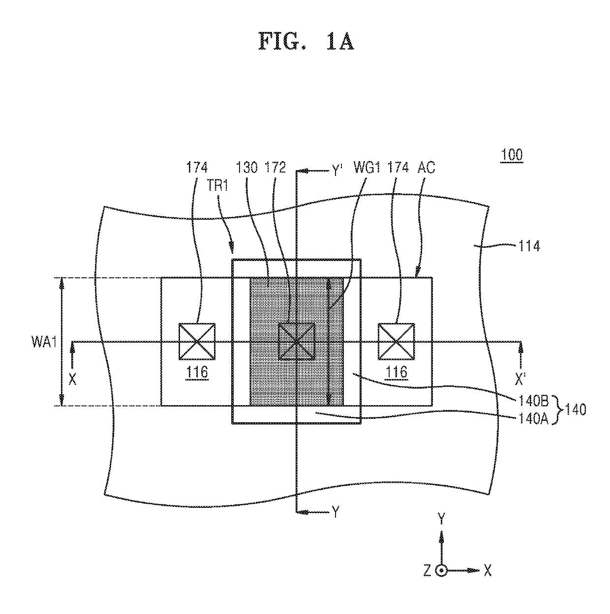
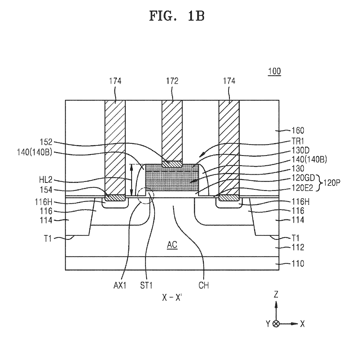
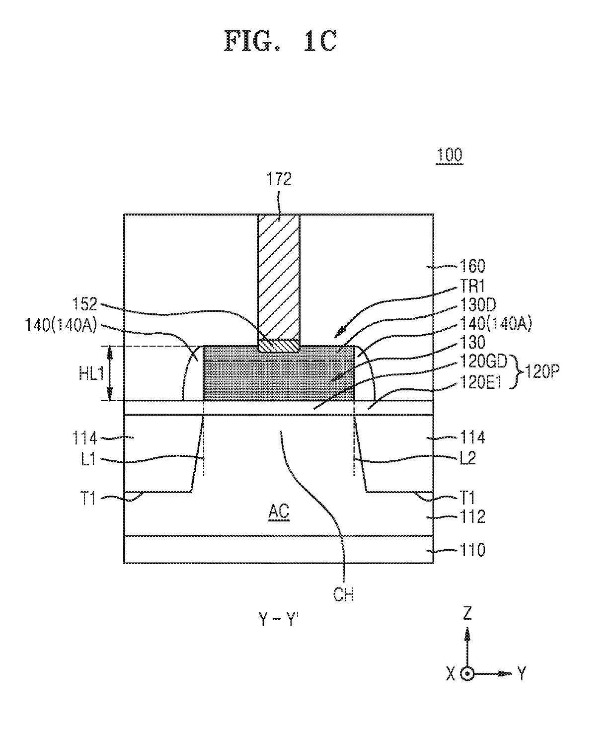
[0019]FIG. 1A is a planar layout diagram of main components of an integrated circuit device according to some embodiments of the inventive concepts, FIG. 1B is a cross-sectional view taken along a line X-X′ of FIG. 1A, and FIG. 1C is a cross-sectional view taken along a line Y-Y′ of FIG. 1A.

[0020]Referring to FIGS. 1A to 1C, an integrated circuit device 100 includes a transistor TR1 formed on a substrate 110 in which a well 112 is formed. The transistor TR1 may be a high-voltage transistor that is configured to operate at a high voltage of about 8 V to about 200 V.

[0021]The substrate 110 includes a trench region T1. An active region AC may be defined in the substrate 110 by the trench region T1 and a device isolation fi...


PUM


Abstract

Integrated circuit devices are provided. An integrated circuit device includes a substrate and a device isolation film on the substrate. An active region of the substrate is defined by the device isolation film on the substrate and has a first width in a horizontal direction. A gate electrode is on the active region and has a second width equal to or less than the first width of the active region in the horizontal direction. The integrated circuit device includes an insulating spacer over the device isolation film and the active region.

Description

CROSS-REFERENCE TO RELATED APPLICATION[0001]This application claims the benefit of Korean Patent Application No. 10-2018-0000899, filed on Jan. 3, 2018, in the Korean Intellectual Property Office, the disclosure of which is hereby incorporated herein in its entirety by reference.BACKGROUND[0002]The present disclosure relates to integrated circuit devices and, more particularly, to integrated circuit devices that include a gate electrode for implementing an analog semiconductor device.[0003]As the degree of integration of integrated circuit devices gradually increases with the development of the electronics industry, it may be beneficial to provide designs that improve the reliability of integrated circuit devices within reduced areas. In particular, display driver integrated circuits (DDIs) for driving display devices, such as liquid crystal display devices (LCDs) or plasma display panels (PDPs), are being developed. DDIs include high-voltage transistors that may operate at a high v...

Claims


Application Information

Patent Timeline
IPC IPC(8): H01L29/08H01L29/06H01L29/423H01L29/45H01L21/762
CPCH01L21/26513H01L21/266H01L29/4933H01L21/32139H01L29/6656H01L21/0274H01L21/32155H01L29/665H01L29/0847H01L29/0653H01L29/42356H01L29/45H01L21/76224H01L29/42364H01L21/3085H01L21/02271H01L21/02164H01L29/7833H01L29/7836H01L29/41758H01L29/0603H01L29/0688H01L29/66568H01L21/28141H01L29/42368H01L29/7823H01L29/7848H01L29/4236H01L21/768
Inventor KIM, MYOUNG-SOO
Owner SAMSUNG ELECTRONICS CO LTD
Why Eureka
Try Eureka