Sense amplifier and semiconductor memory device having the same

a memory device and sense amplifier technology, applied in the direction of dc-amplifiers with dc-coupled stages, amplifiers with semiconductor devices/discharge tubes, instruments, etc., can solve the problems of large size of unstable i/o sense amplifier circuits, and difficulty in sensing voltage differences of amplifier circuits, so as to reduce the sensing time, stably perform amplification operations, and high amplification gain

Active Publication Date: 2009-01-08
SAMSUNG ELECTRONICS CO LTD
View PDF14 Cites 19 Cited by
  • Summary
  • Abstract
  • Description
  • Claims
  • Application Information

AI Technical Summary

Benefits of technology

[0027]The sense amplifier circuit corresponding to a dual sense amplifier implemented with both the current sense amplifier and the voltage sense amplifier has a high amplification gain and stably performs an amplification operation. The sense amplifier circuit according to an exemplary embodiment of the present invention may reduce a sensing time compared with the conventional sense amplifier. Because the dissipation current in the current sense amplifier is significantly decreased after the difference between the differential output voltages is developed and the current sense amplifier may be deactivated after the voltage sense amplifier is enabled, current dissipation may be reduced. The sense amplifier circuit according to an exemplary embodiment of the present invention may guarantee a timing margin for performing the next sensing operation. Moreover, the sense amplifier circuit according to an exemplary embodiment of the present invention does not require an additional differential amplifier. Accordingly, the sense amplifier circuit according to an exemplary embodiment of the present invention may reduce the power consumption and the occupation area in the semiconductor device. Because the current sense amplifier and the voltage sense amplifier included in the sense amplifier circuit according to an exemplary embodiment of the present invention may be activated at different points, the current sense amplifier may stably amplify and generate differential output voltages although active elements may be mismatched with respect to each other.

Problems solved by technology

As the load of an I / O sense amplifier circuit implemented with conventional voltage sense amplifiers is increased, the 110 sense amplifier circuit has difficulties in sensing voltage differences, because a distance between the I / O sense amplifier circuit and a memory cell array becomes longer.
As an amplification gain is increased, an input resistance of the I / O sense amplifier circuit implemented with the current sense amplifiers may have a negative value, and thus the I / O sense amplifier circuit may be unstable.
When, sizes of transistors in the current sense amplifier are increased, however, the sizes of the I / O sense amplifier circuit are significantly increased and a current consumption is also increased.

Method used


Image

  • Sense amplifier and semiconductor memory device having the same
  • Sense amplifier and semiconductor memory device having the same
  • Sense amplifier and semiconductor memory device having the same

Examples


Embodiment Construction

[0045]Exemplary embodiments of the present invention now will be described more fully with reference to the accompanying drawings, in which exemplary embodiments of the invention are shown. The present invention may, however, be embodied in many different forms and should not be construed as limited to the exemplary embodiments set forth herein. Rather, these exemplary embodiments are provided so that this disclosure will be thorough and complete, and will fully convey the scope of the invention to those of ordinary skill in the art. Like reference numerals refer to like elements throughout this application.

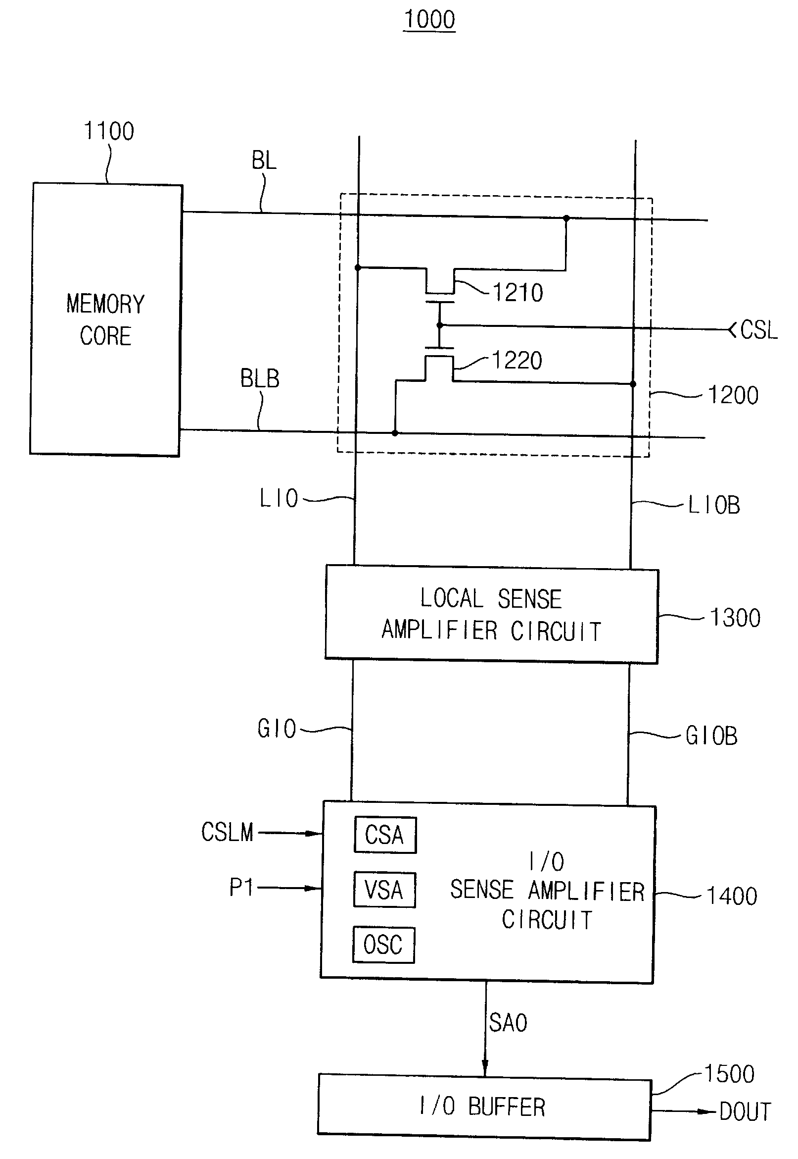
[0046]FIG. 1 is a circuit diagram illustrating a semiconductor device 1000 according to an exemplary embodiment of the present invention. Data output paths of the semiconductor memory device 1000 are illustrated in FIG. 1.

[0047]Referring to FIG. 1, the semiconductor memory device 1000 may include a memory core 1100, a column selection circuit 1200, a local sense amplifier circuit...


PUM


Abstract

A sense amplifier circuit includes a current sense amplifier, a voltage sense amplifier, and an output stabilizing circuit. The current sense amplifier amplifies differential input currents to generate differential output voltages and provides the differential output voltages to a sense amplifier output line pair. The voltage sense amplifier is coupled to the sense amplifier output line pair to amplify the differential output voltages on the sense amplifier output line pair. The voltage sense amplifier is activated at the time later than a time of activation of the current sense amplifier. The output stabilizing circuit is coupled to the sense amplifier output line pair to stabilize the differential output voltages on the sense amplifier output line pair. The output stabilizing circuit has a positive input resistance. Accordingly, the sense amplifier circuit reduces power consumption and an occupied area on a semiconductor chip.

Description

CROSS-REFERENCE TO RELATED APPLICATION[0001]This application claims priority under 35 USC §119 to Korean Patent Application No. 2007-0068226, filed on Jul. 6, 2007, in the Korean Intellectual Property Office (KIPO), the contents of which are incorporated herein in its entirety by reference.BACKGROUND OF THE INVENTION[0002]1. Technical Field[0003]The present disclosure relates to a semiconductor memory device and, more particularly, to a sense amplifier circuit, a semiconductor memory device having a sense amplifier and a method of amplifying a signal.[0004]2. Discussion of Related Art[0005]A semiconductor memory device is used for storing data in various electronic products and applications. A sense amplifier circuit is used during a data input-output (I / O) procedure in the semiconductor memory device. The sense amplifier circuit includes a bit-line sense amplifier circuit amplifying voltages of a bit-line pair, a local sense amplifier circuit amplifying voltages of a local I / O line...

Claims


Application Information

Patent Timeline
Patent Type & Authority Applications(United States)
IPC IPC(8): G11C7/06G01R19/00
CPCG11C7/065G11C7/08G11C7/1048G11C2207/063G11C7/1069G11C2207/005G11C7/1051G11C5/14G11C7/06
Inventor HONG, SANG-PYOLIM, JUN-HEE
Owner SAMSUNG ELECTRONICS CO LTD
Why Eureka
Try Eureka