


Quick Research
Generate reliable direction feasibility study reports for your R&D in just a few steps.

Technical Q&A
Discover and master advanced knowledge NOW. Basics, ideas, possibilities, all at once.

Find Solutions
As an expert in R&D theories, this can generate solutions to your technical problems instantly.

Evaluate Feasibility
Analyze your overall solution with one click, know your potential R&D risks in advance.

Monitor Landscape
Get weekly tech updates, stay abreast of the latest tech innovations and key insights.
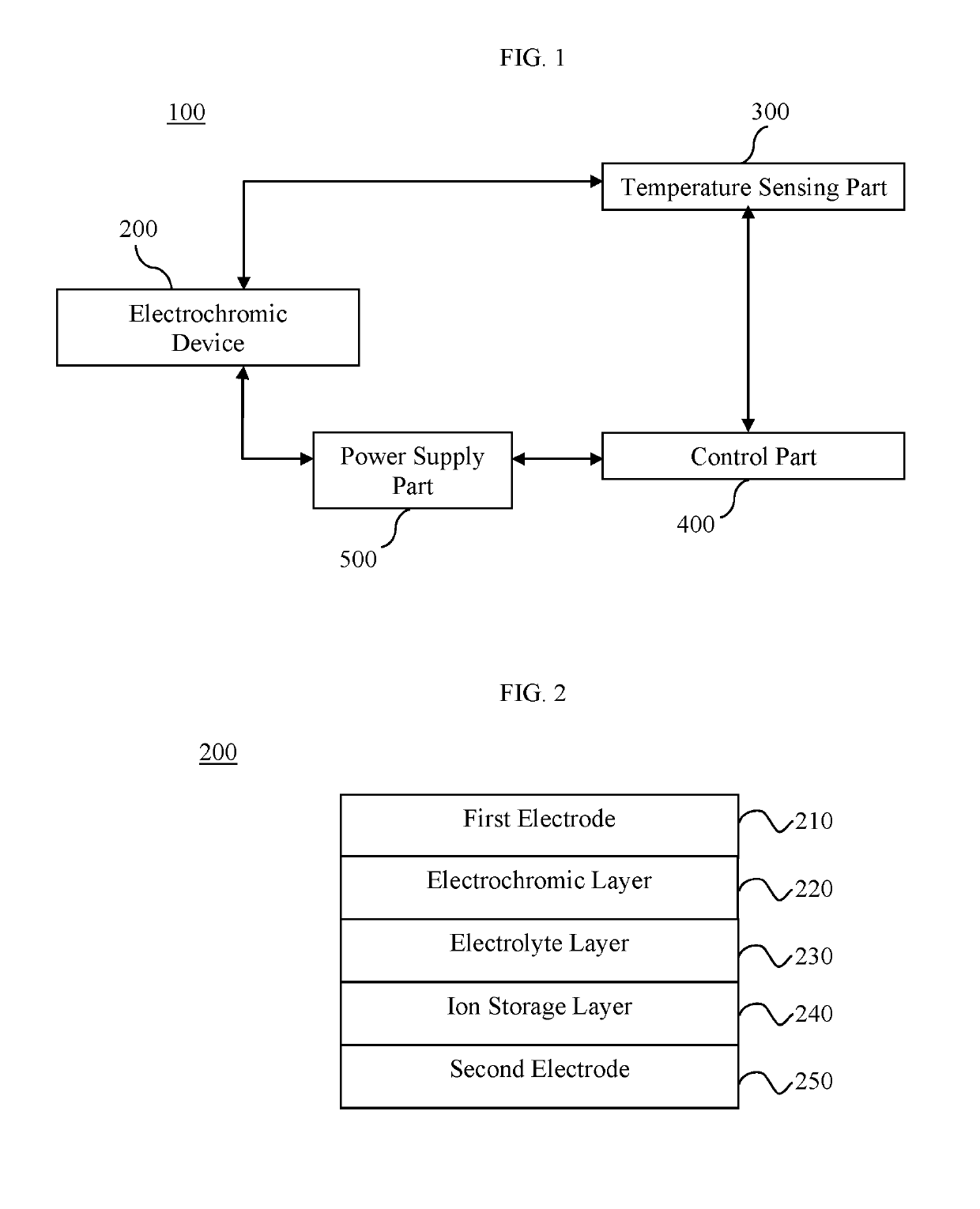
Electrochromic module and driving method for electrochromic device
a technology of electrochromic devices and electrochromic modules, applied in static indicating devices, instruments, non-linear optics, etc., can solve the problems of low power consumption, slow response speed of electrochromic devices, and low power consumption, so as to improve the durability of electrochromic devices
- Summary
- Abstract
- Description
- Claims
- Application Information
AI Technical Summary
Benefits of technology
Problems solved by technology
Method used
Image

Examples
production example 1
ode (Half-Cell)
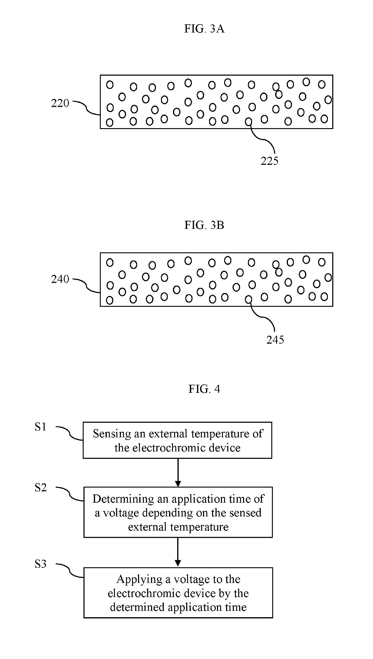
[0056]A coating solution comprising tungsten oxide (WO3) particles was applied to an Indium tin oxide / polyethylene terephthalate (ITO / PET) base material and heat-treated to form an electrochromic layer having a thickness of 300 nm. The coating solution was applied by a bar coating method and then heat-treated at 130° C. for 3 minutes. At this time, the area of the electrode was set to 20 cm2 (4 cm×5 cm). When the produced half-cell is colored from a bleached state at a voltage of 0.7 V and room temperature (RT), light transmittance upon coloring may be changed to 70 to 80%.
production example 2
[0057]An electrode was produced in the same manner as in Production Example 1, except that an ion storage layer comprising PB particles was formed. When the produced half-cell is colored from a bleached state at a voltage of 0.7 V and room temperature (RT), light transmittance upon coloring may be changed to 70 to 80%.
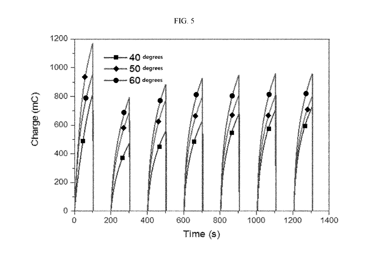
[0058]Measurement of Optimum Reaction Charge Amount
[0059]When the voltage is continuously applied even after the color-switching of the electrochromic material is completed, an additional reaction and chemical degradation occur to decrease the durability of the electrochromic device, and thus, the charge amount supplied at the time when the color-switching is completed can be regarded as the optimum reaction charge amount. At this time, the time when the color-switching of the electrochromic material is completed may mean a time when 90% of the minimum light transmittance upon coloring is reached, if each half-cell as produced below is colored fr...
PUM
| Property | Measurement | Unit |
|---|---|---|
| diameter | aaaaa | aaaaa |
| thickness | aaaaa | aaaaa |
| temperature | aaaaa | aaaaa |
Abstract
Description
Claims
Application Information
 - R&D Engineer
- R&D Manager
- IP Professional
- Industry Leading Data Capabilities
- Powerful AI technology
- Patent DNA Extraction
Browse by: Latest US Patents, China's latest patents, Technical Efficacy Thesaurus, Application Domain, Technology Topic, Popular Technical Reports.
© 2024 PatSnap. All rights reserved.Legal|Privacy policy|Modern Slavery Act Transparency Statement|Sitemap|About US| Contact US: help@patsnap.com