

Display device
Active Publication Date: 2019-08-08
SHARP KK
View PDF11 Cites 4 Cited by
- Summary
- Abstract
- Description
- Claims
- Application Information
AI Technical Summary
Benefits of technology
[0011]Thus, the following disclosure aims to realize a low-cost display device capable of suppressing occurrence o
Problems solved by technology
Further, if the device is turned on in a state in which a residual charge is accumulated within the pixel formation portion, display defect such as flicker may occur due to an unevenness of impurities based on the residual charge.
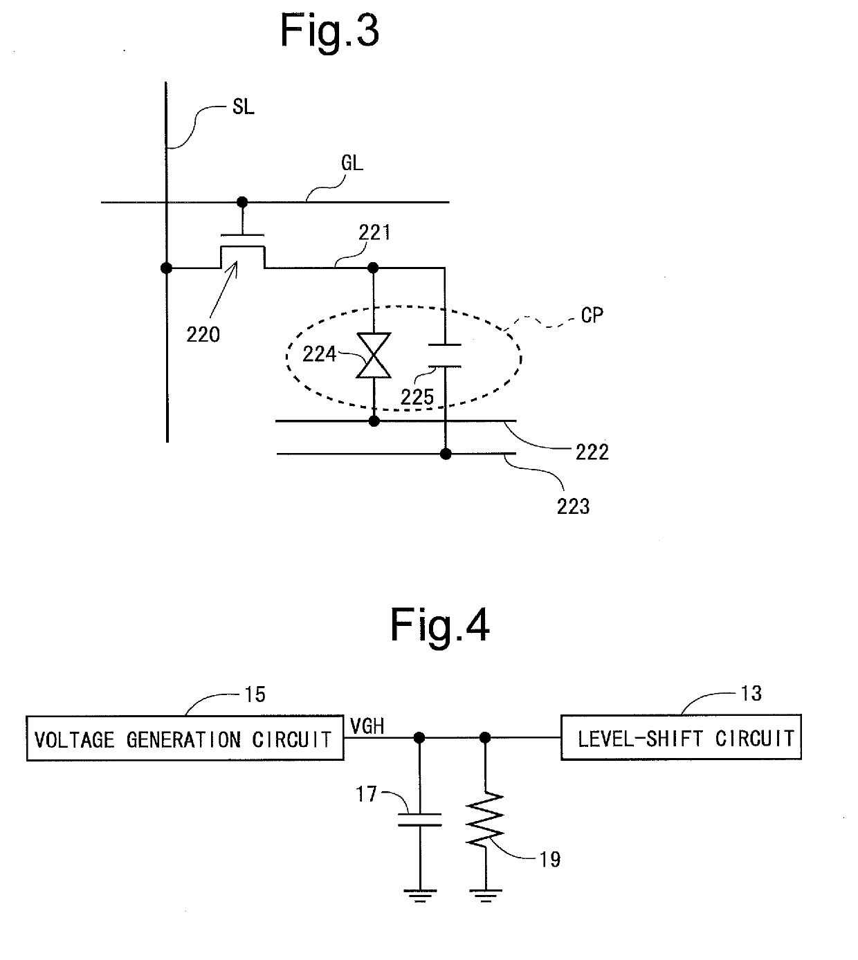
As can be seen from FIG. 20, regarding the a-SiTFT and the LTPS-TFT, off characteristics are not good (an off leakage current is relatively high).
Accordingly, in a case in which IGZO-TFT liquid crystal panel employed, electric charges are not sufficiently discharged within a period, for example, until the scanning lines become an unselected stage when the power supply is sto
Method used
View moreImage
Smart ImageViewing Examples

Examples
 PUM
 Abstract
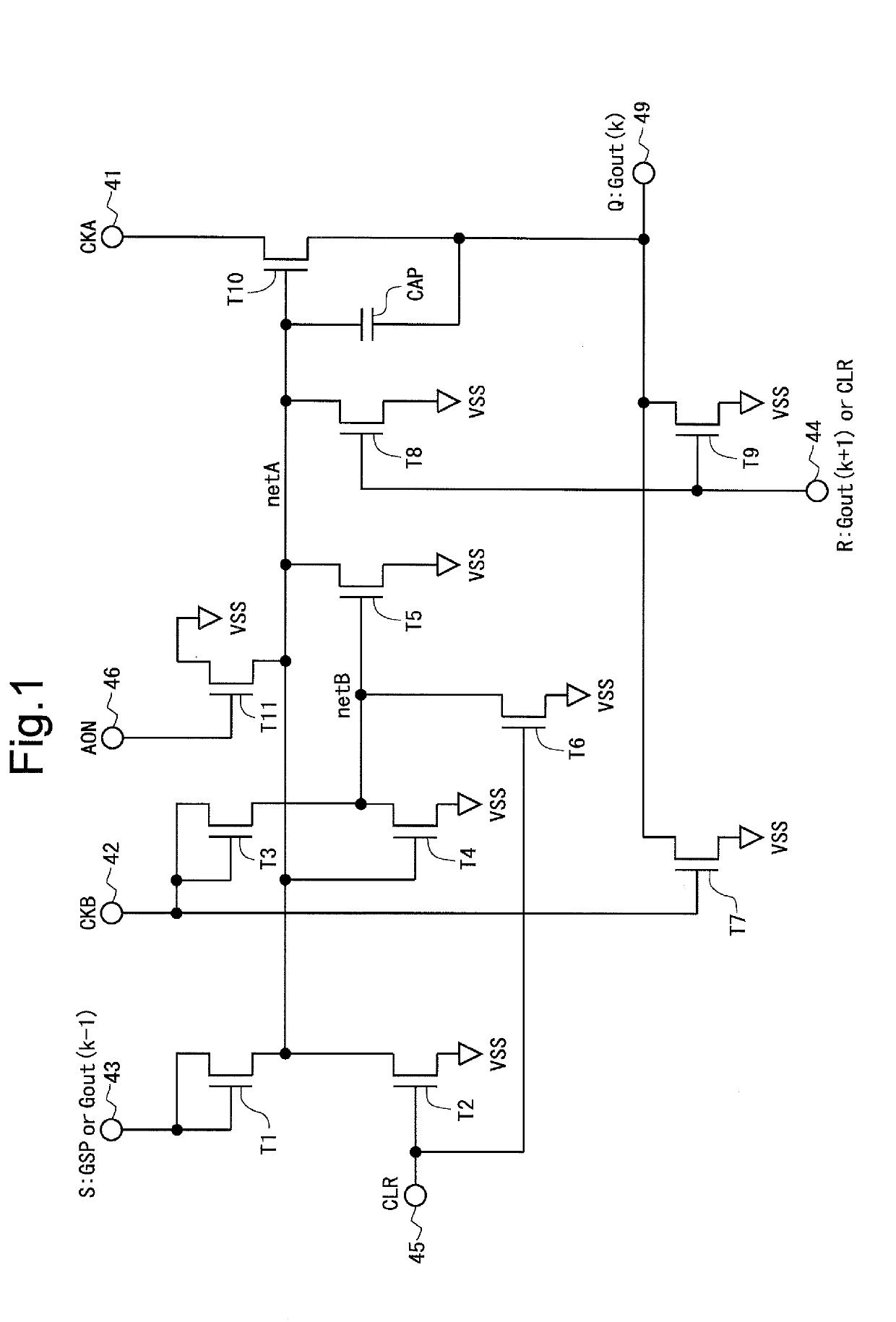
A configuration in which a voltage (a gate on voltage) of only one system is used as a voltage for turning scanning lines to a selected state is employed (single power supply system configuration). A unit circuit that constitutes a shift register within a gate driver includes a thin film transistor whose source terminal is connected to an output control node. In such a configuration, when the external power supply is stopped, a voltage supplied to a gate terminal of the thin film transistor and a voltage supplied to a drain terminal of the thin film transistor are set to the gate on voltage.
Description
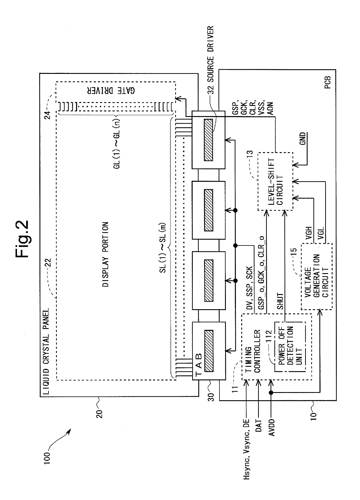
BACKGROUND OF THE INVENTION1. Field of the Invention[0001]The present invention relates to a display device, and in particular to processing when external power supply is stopped.2. Description of Related Art[0002]In general, an active matrix-type liquid crystal display device includes a liquid crystal layer and a liquid crystal panel constituted by two substrates that hold the liquid crystal layer. One of the two substrates is provided with a plurality of scanning lines, a plurality of data lines, and a plurality of pixel formation portions arranged in a matrix so as to correspond to respective intersections between the plurality of scanning lines and the plurality of data lines. Each of the pixel formation portions includes a thin film transistor (TFT) whose gate terminal is connected to a scanning line that passes a corresponding intersection and whose source terminal is connected to a data line that passes the same intersection, a pixel capacitance to which a data signal that is...
Claims
Login to View More Application Information
Patent Timeline
 IPC IPC(8): G09G3/36
CPCG09G2310/0286G09G2310/08G09G2320/0247H01L27/1225G09G2310/0251G09G3/3696G02F1/1368G02F2202/10G09G3/3677G11C19/28G09G2330/027G09G2310/063G09G2320/0233G09G2320/0257G09G2320/0204
InventorKUSUMI, TAKATSUGUWATANABE, TAKUYATAGAWA, AKIRAIWASE, YASUAKITAKEUCHI, YOHEI
OwnerSHARP KK