Supercharge Your Innovation With Domain-Expert AI Agents!

Techniques for command synchronization in a memory device

a memory device and command synchronization technology, applied in the field of memory devices, can solve the problems of incorrect read data provided by the memory, inadvertently ignored read commands, incorrect write data provided,

Active Publication Date: 2019-08-08
MICRON TECH INC
View PDF12 Cites 9 Cited by
  • Summary
  • Abstract
  • Description
  • Claims
  • Application Information

AI Technical Summary

Benefits of technology

The patent text describes a system for synchronizing command signals in memory devices. The technical effect of the patent is to ensure that command signals and internal clock signals are properly timed in memory devices, so that data is output correctly and without being ignored or incorrect. The patent also discusses the issue of latency, or the time between receipt of a read or write command and the output of data, and how to address this issue to maintain proper timing. The patent proposes various circuits and methods for achieving command synchronization in memory devices, while reducing power consumption and improving efficiency.

Problems solved by technology

If the timing of the internal read command signal is not such that the data path circuitry is enabled at the time the internal clock signal clocks the data path circuitry to output the read data at an expected time, the read command may be inadvertently ignored or the read data provided by the memory may not be correct (e.g., the data associated with another read command).
Inaccurate timing of the internal command and clock signals could result in the write command being inadvertently ignored or incorrect write data being provided to the memory device (e.g., the write data is associated with another write command).
As appreciated, the higher the frequency of the clock signals in memory devices, the more challenging it may be to generate correctly timed internal clock and command signals.

Method used


Image

  • Techniques for command synchronization in a memory device
  • Techniques for command synchronization in a memory device
  • Techniques for command synchronization in a memory device

Examples


Embodiment Construction

[0022]One or more specific embodiments will be described below. In an effort to provide a concise description of these embodiments, not all features of an actual implementation are described in the specification. It should be appreciated that in the development of any such actual implementation, as in any engineering or design project, numerous implementation-specific decisions must be made to achieve the developers' specific goals, such as compliance with system-related and business-related constraints, which may vary from one implementation to another. Moreover, it should be appreciated that such a development effort might be complex and time consuming, but would nevertheless be a routine undertaking of design, fabrication, and manufacture for those of ordinary skill having the benefit of this disclosure.

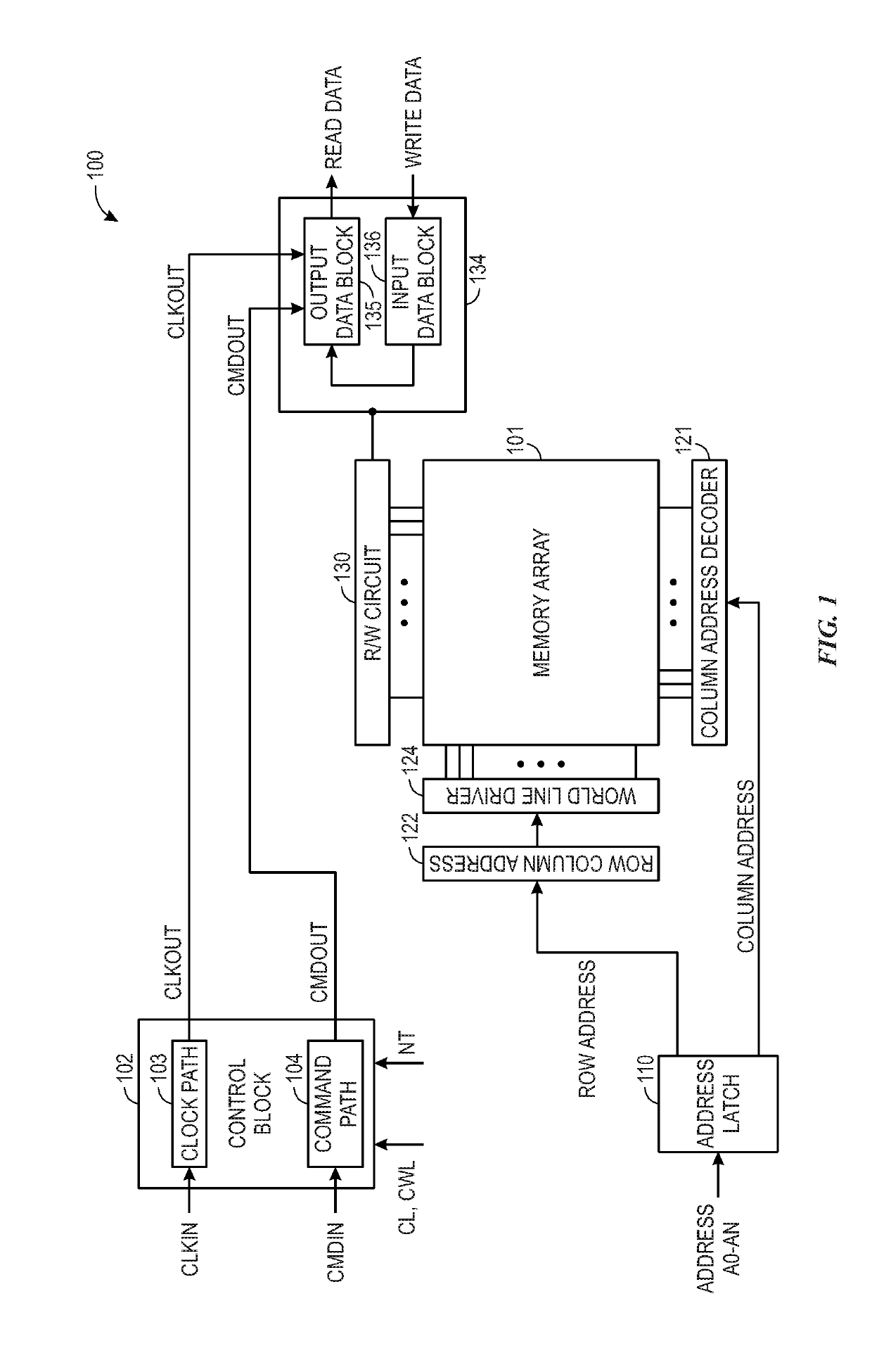
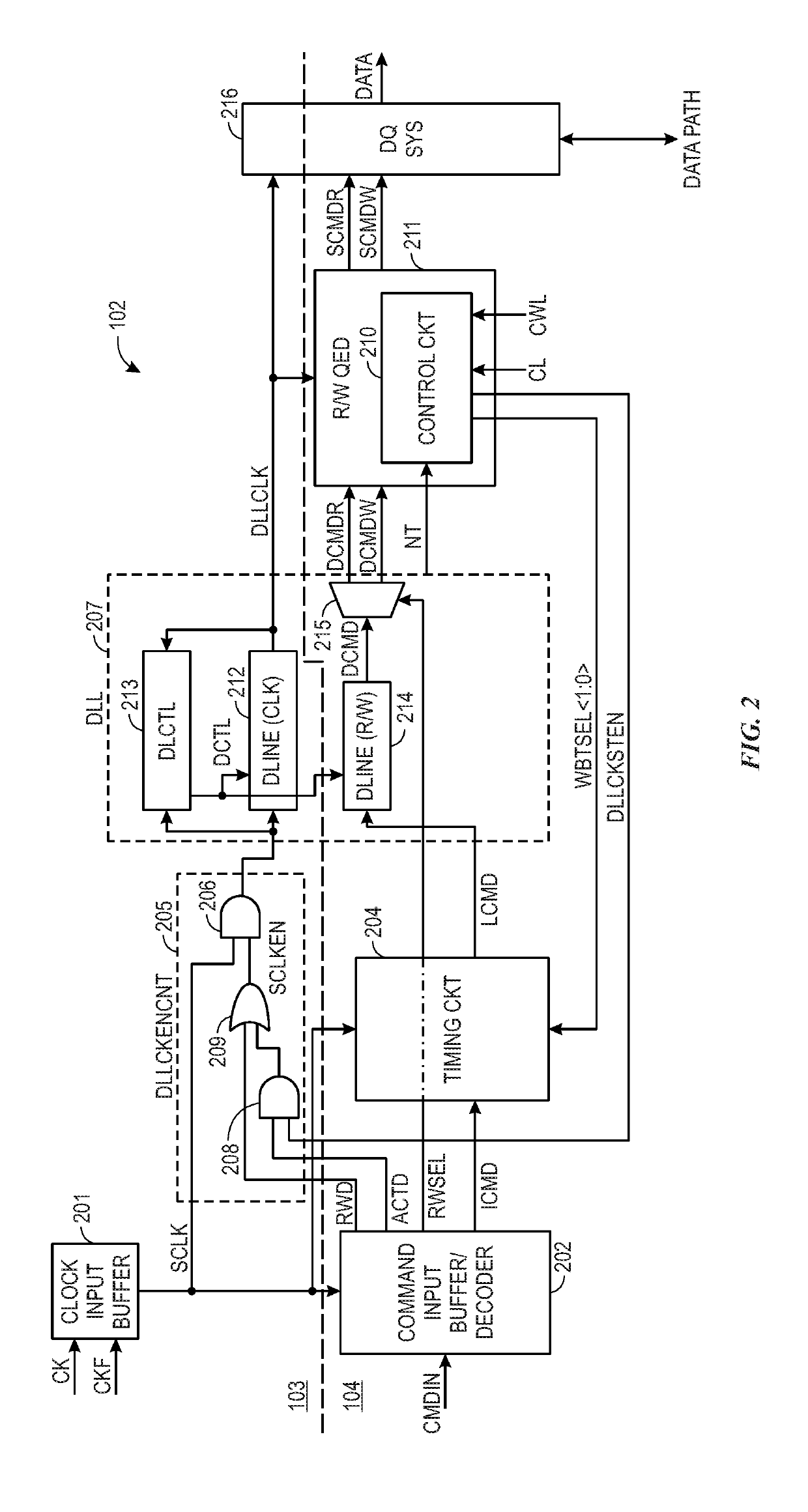
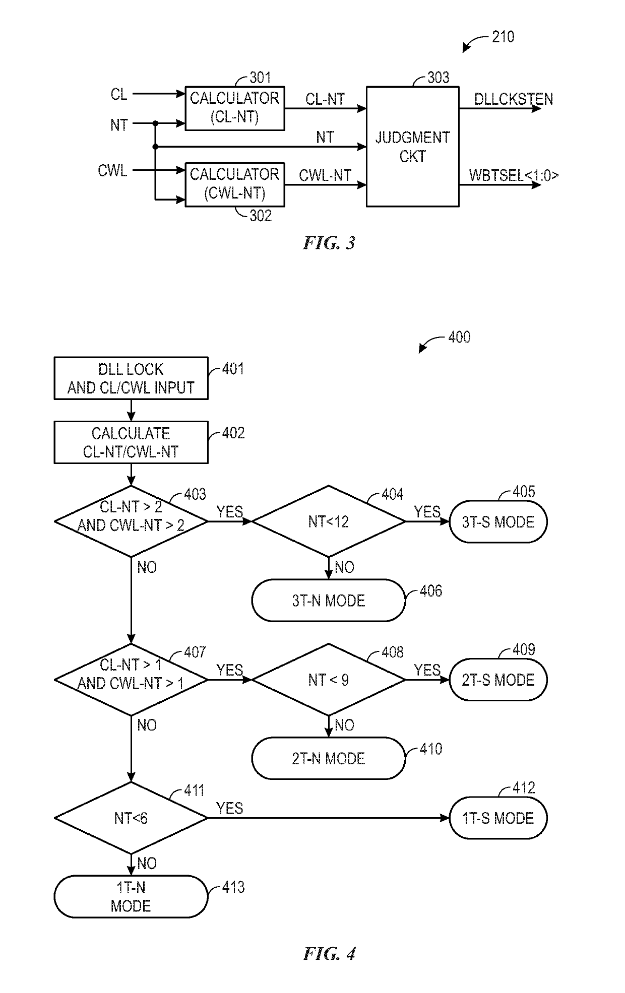
[0023]As is described in detail below, memory devices may employ circuits and techniques to synchronize various internal signals with an internal clock signal to ensure proper fun...


PUM


Abstract

An apparatus, such as a memory device, that includes circuits and techniques to synchronize various internal signals with an internal clock signal to ensure proper functionality of the memory device through various modes of operation. A clock enable control circuit is provided to control the input of a delay locked loop circuit to provide a locked condition based on a particular type of command input and the state of various control signals to allow for multiple locking conditions and adjustments based on a length of a clock cycle of the internal clock signal.

Description

BACKGROUND[0001]Embodiments described herein relate generally to the field of memory devices. More specifically, the current embodiments include one or more systems, devices, and methods for command synchronization in memory devices.DESCRIPTION OF RELATED ART[0002]This section is intended to introduce the reader to various aspects of art that may be related to various aspects of the present disclosure, which are described and / or claimed below. This discussion is believed to be helpful in providing the reader with background information to facilitate a better understanding of the various aspects of the present disclosure. Accordingly, it should be understood that these statements are to be read in this light, and not as admissions of prior art.[0003]In semiconductor memory, proper operation of the memory device is based on the correct timing of various internal command and clock signals. For example, in reading data from the memory device, internal clock signals that clock data path ...

Claims


Application Information

Patent Timeline
Patent Type & Authority Applications(United States)
IPC IPC(8): G11C7/22G11C8/10
CPCG11C7/222G11C8/10G11C7/225H03L7/08G11C7/1045G11C7/1066G11C7/106H03L7/0812
Inventor KOMATSU, YOSHIYAMIYANO, KAZUTAKAMOMMA, ATSUKO
Owner MICRON TECH INC
Features
  • R&D
  • Intellectual Property
  • Life Sciences
  • Materials
  • Tech Scout
  • Unparalleled Data Quality
  • Higher Quality Content
  • 60% Fewer Hallucinations
Learn More