Method of processing a wafer

a technology of processing method and wafer, which is applied in the direction of manufacturing tools, soldering devices, and auxillary welding devices, etc., can solve the problems of uneven front side of the wafer, ineffective protection of the surface, and uneven surface profile, so as to reduce the thickness of the wafer, and protect the surface from damage. , the effect of compromising the quality of the resultant chips or dies

Active Publication Date: 2019-08-15
DISCO CORP
View PDF1 Cites 2 Cited by
  • Summary
  • Abstract
  • Description
  • Claims
  • Application Information

AI Technical Summary

Benefits of technology

[0143]If the cushioning layer is attached to the back surface of the protective film, such protrusions or projections can be embedded in the cushioning layer. Hence, any negative influence of the surface unevenness arising from the presence of the protrusions on subsequent wafer processing steps, such as grinding and / or cutting, can be eliminated. In particular, the cushioning layer can significantly contribute to achieving a particularly uniform and homogeneous distribution of pressure during grinding and cutting processes.
[0144]By embedding the protrusions in the cushioning layer, the protrusions, such as, for example, bumps, optical elements or other structures, are reliably protected from any damage during wafer processing, for example, in a subsequent grinding or cutting step.
[0145]Further, if the wafer is ground to a small thickness in a grinding step, e.g., a thickness in the pm range, protrusions present on the wafer front side, e.g., in the device area, may cause a deformation of the wafer back side, due to the reduced thickness of the wafer and the pressure applied thereto in the grinding process. This latter effect is referred to as “pattern transfer”, since the pattern of the protrusions on the wafer front side is transferred to the wafer back side, and results in an undesired unevenness of the back side surface of the wafer, thus compromising the quality of the resulting chips or dies.
[0146]The protective film and the cushioning layer act as a cushion or buffer between the wafer front side and, for example, a support or carrier on which the wafer front side rests during processing, e.g., grinding and / or polishing, the wafer back side, thus contributing to achieving a uniform and homogeneous distribution of pressure during processing. Hence, a pattern transfer or breakage of the wafer during processing, in particular, grinding, the back side thereof can be particularly reliably prevented.

Problems solved by technology

The division lines partitioning these devices may form at least slight grooves or trenches between the devices, thus resulting in an uneven surface profile.
Also such partial cuts introduce a surface profile which renders the wafer front side uneven.
When attaching a protective film or sheeting to such an uneven wafer surface in a conventional manner, problems arise in that, e.g., due to the presence of grooves, trenches or protrusions, the surface is not efficiently protected.
In particular, the protective film may not reliably seal the wafer surface at a peripheral wafer portion, allowing contaminants, such as debris, grinding water or cutting water, to enter and contaminate the surface.
In known semiconductor device fabrication processes, problems may arise during the process of grinding wafers to such small thicknesses, in particular, at high speed.
Specifically, the grinding process may cause the formation of sharp wafer edges which act as starting points for wafer chipping and breakage, thus significantly affecting the quality of the resulting chips or dies.
Further, equipment used for dividing the wafer after grinding, such as a blade or a saw, may be damaged due to being impacted by loose, small-sized chips arranged at the peripheral wafer portion.
Such sharp wafer edges may also lead to problems in the storage and / or transport of ground wafers, e.g., damaging the containers in which they are received, such as wafer cassettes or the like.
However, the requirement of an additional edge trimming step renders the wafer processing method more complicated and reduces the processing efficiency.

Method used


Image

  • Method of processing a wafer
  • Method of processing a wafer
  • Method of processing a wafer

Examples


first embodiment

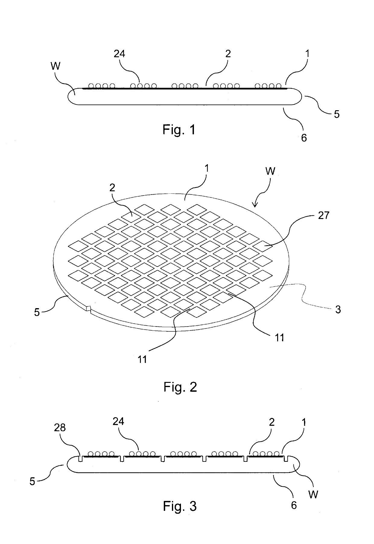
[0198]In the following, a method of processing a wafer W according to the present invention will be described with reference to FIGS. 1 to 10B.

[0199]FIG. 1 shows a cross-sectional view of the wafer W to be processed by the method of the present invention. FIG. 2 shows a perspective view of the wafer W shown in cross-section in FIG. 1.

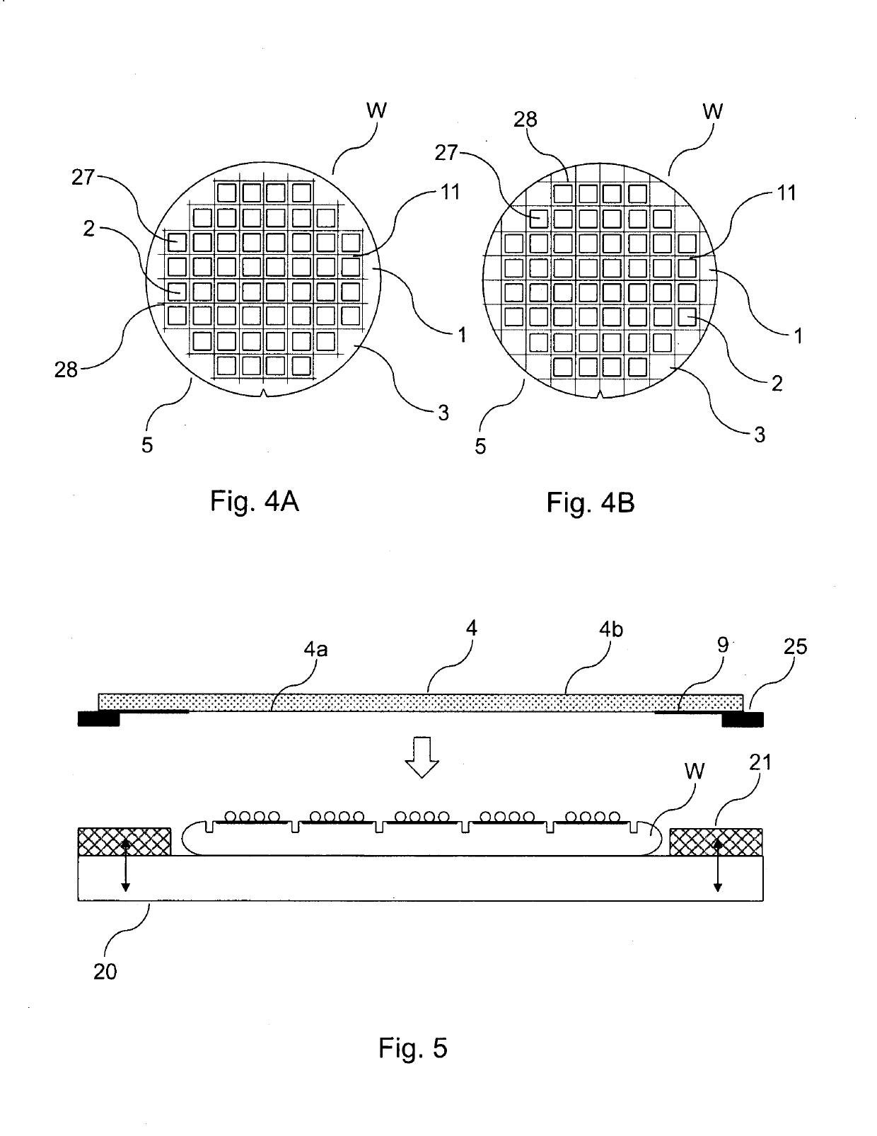
[0200]In the method of this embodiment, as a first step, wafer material is removed along the division lines 11 (see FIGS. 4A and 4B) from the front side 1 of the wafer W. In this process, wafer material is removed along only a part of the thickness of the wafer W so as to form grooves 28 extending along the division lines 11, as is shown in FIGS. 3, 4A and 4B.

[0201]The wafer material may be removed along the division lines 11 in the manner detailed above. In particular, the wafer material may be mechanically removed along the division lines 11. For example, the wafer material may be removed along the division lines 11 by mechanically cutting the wafer W...

second embodiment

[0255]In the following, a method of processing the wafer W according to the present invention will be described with reference to FIGS. 11 and 12.

[0256]In the description of the second embodiment, the elements which are similar or identical to those of the first embodiment are denoted by the same reference signs and a repeated detailed description thereof is omitted.

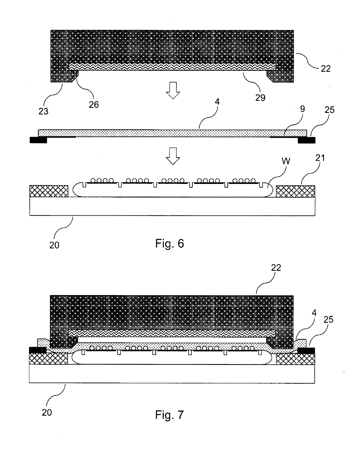
[0257]The wafer processing method according to the second embodiment substantially only differs from the wafer processing method according to the first embodiment in that the annular frame 25 is omitted (see FIGS. 11 and 12). Further, in the second embodiment, the outer diameter of the protective film 4 is smaller than in the first embodiment.

[0258]In particular, the outer diameter of the protective film 4 of the second embodiment is smaller than the outer diameter of the pressing stamp 22. However, also the outer diameter of the protective film 4 of the second embodiment is larger than the outer diameter of the wafer W,...


PUM

PropertyMeasurementUnit
thicknessesaaaaaaaaaa
temperatureaaaaaaaaaa

Abstract

A method of processing a wafer having on one side a device area with a plurality of devices includes providing a protective film and applying the protective film to the device side of the wafer or to the other side of the wafer, so that at least a central area of a front surface of the protective film is in direct contact with the device side or the other side of the wafer. The protective film is attached to the device side or to other side of the wafer, so that at least a part of a peripheral portion of the protective film is attached to at least a part of a lateral edge of the wafer along the entire circumference of the wafer. The lateral edge of the wafer extends from the device side of the wafer to the other side of the wafer.

Description

TECHNICAL FIELD[0001]The present invention relates to a method of processing a wafer, such as a semiconductor wafer, having on one side a device area with a plurality of devices.TECHNICAL BACKGROUND[0002]In a semiconductor device fabrication process, a wafer having a device area with a plurality of devices, commonly partitioned by a plurality of division lines, is divided into individual dies. This fabrication process generally comprises a grinding step for adjusting the wafer thickness and a cutting step of cutting the wafer along the division lines to obtain the individual dies. The grinding step is performed from a back side of the wafer which is opposite to a wafer front side on which the device area is formed. Moreover, also other processing steps, such as polishing and / or etching, may be carried out on the back side of the wafer. The wafer may be cut along the division lines from its front side or its back side.[0003]In order to protect the wafer back side or front side, in pa...

Claims


Application Information

Patent Timeline
Patent Type & Authority Applications(United States)
IPC IPC(8): H01L21/78H01L21/304B23K26/40H01L21/683
CPCH01L21/78H01L21/304B23K26/40H01L21/6836B23K2101/40H01L2221/68331H01L21/67132B23K10/00B23K26/38B23K26/402B23K26/18B23K26/364B23K2103/52B23K2103/54B23K37/0408H01L2221/6834H01L2221/68327H01L21/56H01L21/324H01L21/02013
Inventor PRIEWASSER, KARL HEINZZIMMERMANN, ROLANDHOSHINO, HITOSHI
Owner DISCO CORP
Why Eureka
Try Eureka