A method for processing silicon material

a silicon material and processing method technology, applied in the direction of sustainable manufacturing/processing, semiconductor devices, climate sustainability, etc., can solve the problems of reducing the performance of solar cells, and cid reducing the efficiency of perc solar cells, so as to reduce the loss of photovoltaic devices performance and mitigate the effect of cid

Active Publication Date: 2019-08-15
NEWSOUTH INNOVATIONS PTY LTD
View PDF0 Cites 0 Cited by
  • Summary
  • Abstract
  • Description
  • Claims
  • Application Information

AI Technical Summary

Benefits of technology

The patent is about a method for improving the performance of solar cells by reducing the contact resistance between the metallic electrodes and silicon material. The method involves annealing the substrate at a high temperature for a certain period of time, and exposing it to radiation to control the charge state of hydrogen atoms. The method has been found to stabilize the performance of the solar cells and reduce the loss of performance due to CID (contact induced diode) through a combination of tailored annealing temperatures and exposure to radiation. The technical effects of the patent are an improved stability and efficiency of solar cells throughout their operational life.

Problems solved by technology

Generally, the performance of a solar cell degrades when it is exposed to radiation or more broadly, subject to carrier injection.
CID reduces the efficiency of PERC solar cells and it is known to occur much faster with increasing illumination intensities or at elevated temperatures.
For example, it has been reported that eliminating the contact firing step during manufacturing largely reduces the effects of CID on cell performance.
However, the solutions proposed are either not compatible with cell manufacturing processes, or provide limited improvement.

Method used


Image

  • A method for processing silicon material
  • A method for processing silicon material
  • A method for processing silicon material

Examples


Embodiment Construction

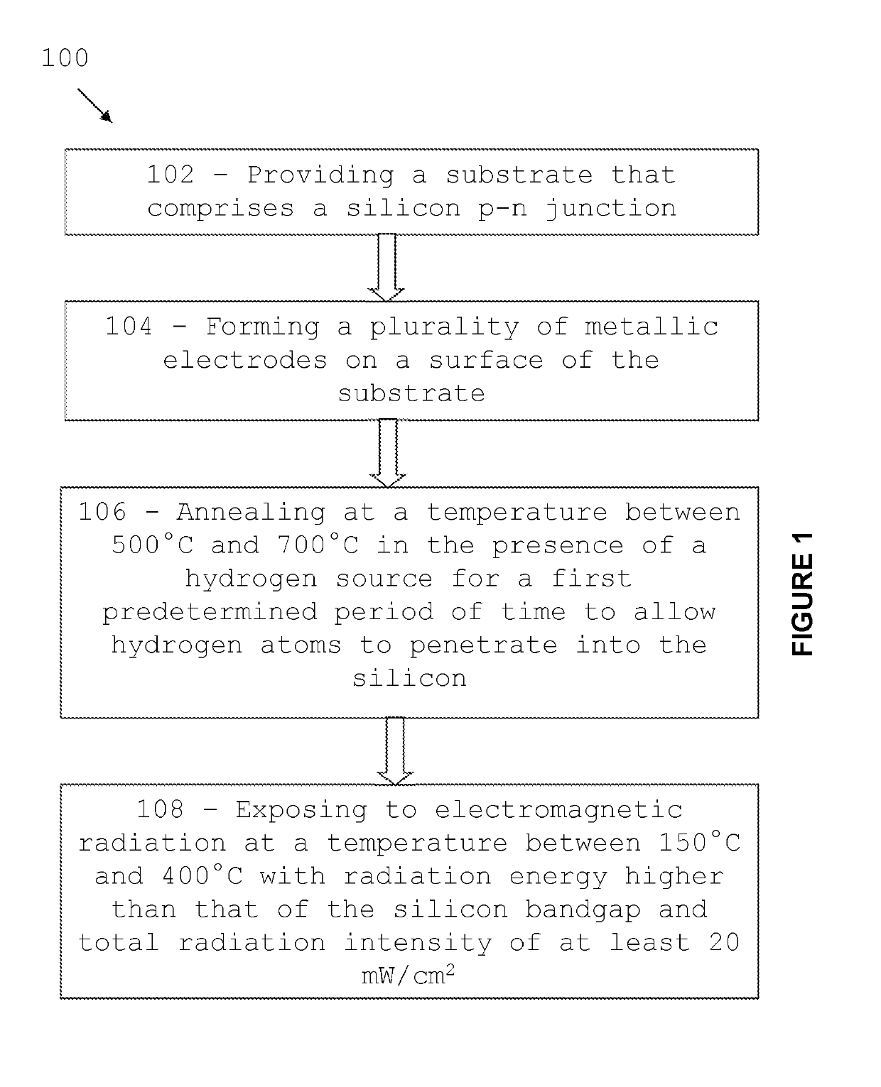
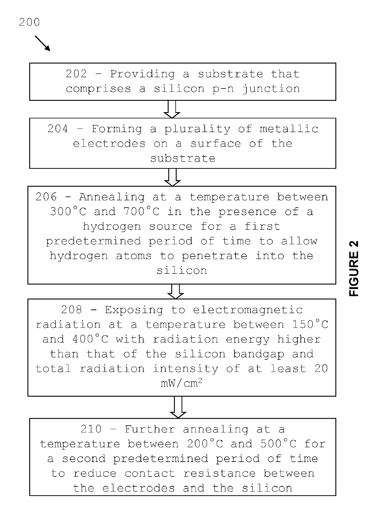
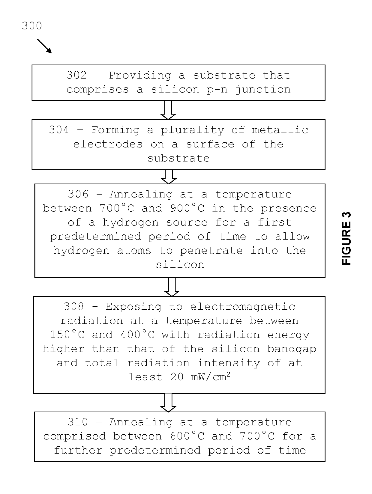
[0052]Embodiments of the present invention generally relate to methods for manufacturing photovoltaic devices and methods for stabilising the performance of photovoltaic devices.

[0053]In the methods described herein, multiple annealing treatments are used in specific order, in conjunction with exposure to radiation, to minimise the effect of CID on the performance of photovoltaic devices. The combined approach disclosed herein provides better stabilised performance over methods that use either heat treatments or radiation treatments.

[0054]Referring now to FIG. 1, there is shown a flow diagram 100 with a series of method steps required to manufacture a photovoltaic device in accordance with embodiments. The photovoltaic device can be any type of solar cell device for example: a screen printed solar cell, non-screen printed solar cell, PERC cell or plated solar cell where the substrate can be a p-type, n-type, mono- or multi-crystalline silicon substrate. After providing a substrate c...


PUM

PropertyMeasurementUnit
temperatureaaaaaaaaaa

Abstract

The present disclosure provides methods for manufacturing a photovoltaic device that comprise a sequence of annealing steps and exposure to electromagnetic radiation during annealing that allow passivating electrically active defects and stabilising the performance of photovoltaic device.

Description

FIELD OF THE INVENTION[0001]The present invention generally relates to methods for manufacturing photovoltaic devices and methods for stabilising the performance of photovoltaic devices.BACKGROUND OF THE INVENTION[0002]Silicon is the main semiconductor material used to fabricate today's commercial solar cells. The majority of commercial solar cells are fabricated from a monocrystalline or multi-crystalline silicon wafer. A p-n junction is formed in the silicon wafer by, for example, diffusing n-type atoms into a p-type silicon wafer.[0003]A large proportion of solar cells are fabricated using a boron-doped wafer (p-type). Generally, the performance of a solar cell degrades when it is exposed to radiation or more broadly, subject to carrier injection. These phenomena are known in the art as Light Induced Degradation (LID) and Carrier Induced Degradation (CID).[0004]In the photovoltaic industry, Passivated Emitter Rear Contact (PERC) solar cells are becoming increasingly popular becau...

Claims


Application Information

Patent Timeline
Patent Type & Authority Applications(United States)
IPC IPC(8): H01L31/18H01L31/068H01L31/0224
CPCH01L31/1864H01L31/1868H01L31/068H01L31/1804H01L31/022425Y02E10/547Y02P70/50H01L31/02167Y02E10/546
Inventor WENHAM, STUART ROSSCIESLA, ALISONHALLAM, BRETT JASONCHAN, CATHERINE EMILYCHONG, CHEE MUNCHEN, RANABBOTT, MALCOLM DAVIDPAYNE, DAVID NEIL
Owner NEWSOUTH INNOVATIONS PTY LTD
Why Eureka
Try Eureka