Method for depositing and reflow of a high quality etch resistant gapfill dielectric film

a dielectric film, high-quality technology, applied in the direction of coatings, chemical vapor deposition coatings, metallic material coating processes, etc., can solve the problem of photolithography's trend for smaller feature sizes, and achieve the effect of reducing the cost of photolithography

Active Publication Date: 2019-08-22
MICROMATERIALS LLC
View PDF0 Cites 33 Cited by
  • Summary
  • Abstract
  • Description
  • Claims
  • Application Information

AI Technical Summary

Problems solved by technology

However, there are demands and device trends for smaller feature sizes not obtainable by photolithography.

Method used


Image

  • Method for depositing and reflow of a high quality etch resistant gapfill dielectric film
  • Method for depositing and reflow of a high quality etch resistant gapfill dielectric film
  • Method for depositing and reflow of a high quality etch resistant gapfill dielectric film

Examples


Embodiment Construction

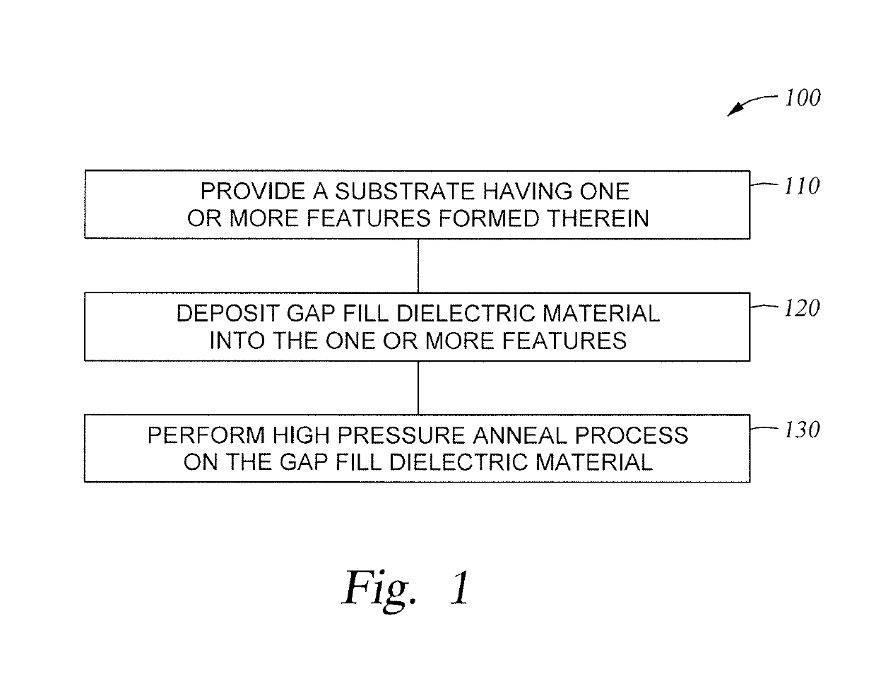
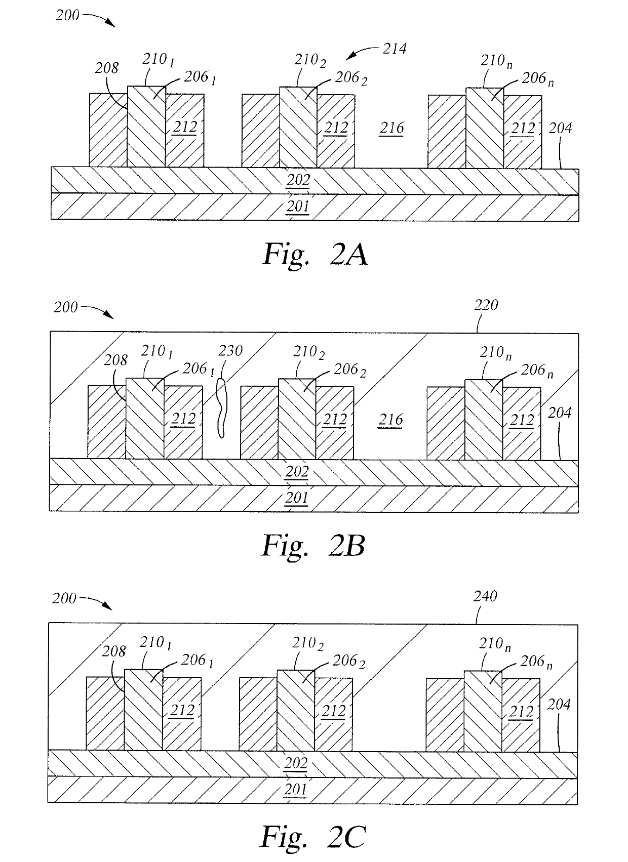
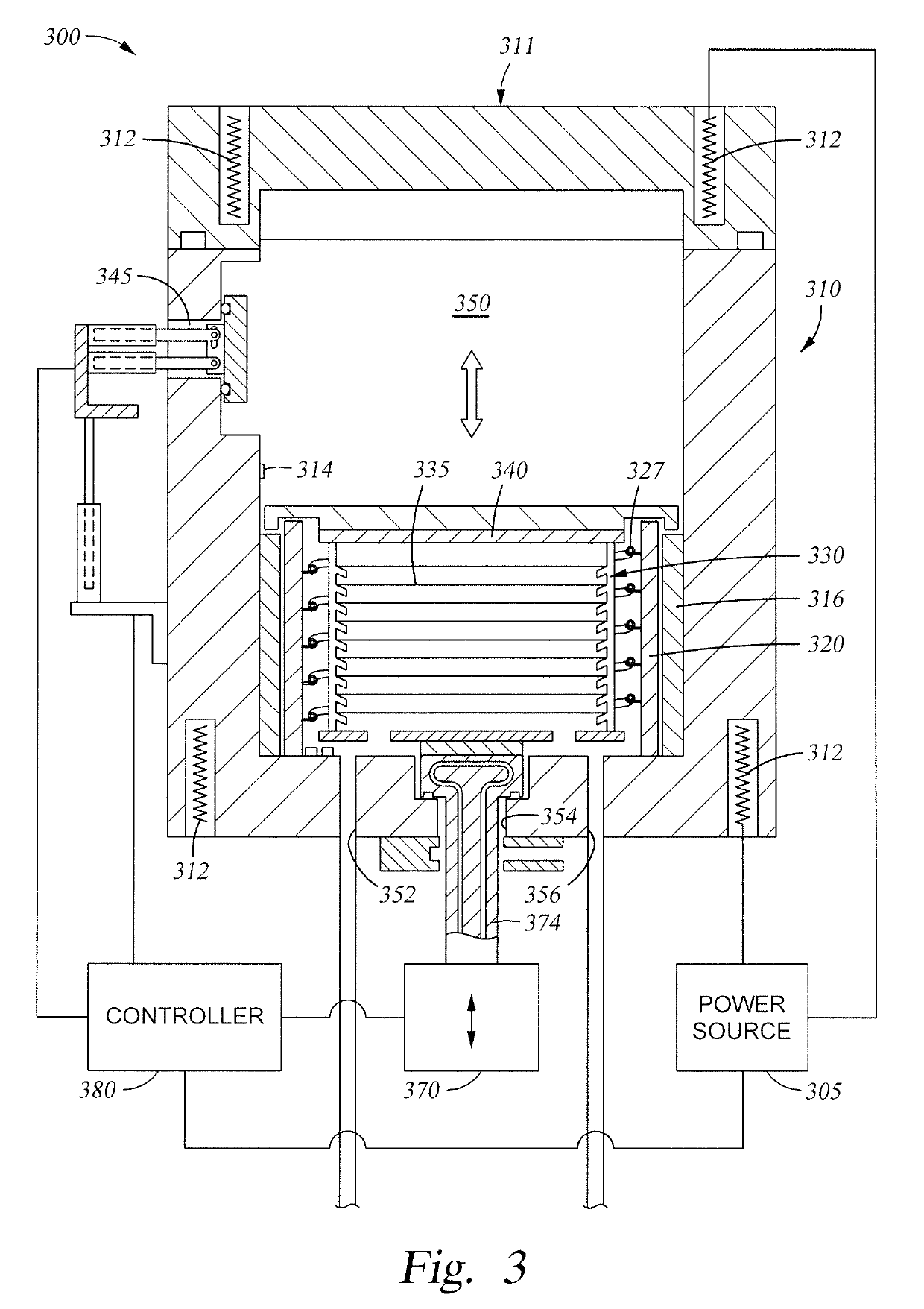
[0015]The following disclosure describes high-pressure annealing processes that may be used to cure defects in gapfill dielectric films. Certain details are set forth in the following description and in FIGS. 1-3 to provide a thorough understanding of various implementations of the disclosure. Other details describing well-known structures and systems often associated with deposition of gapfill dielectric films and high-pressure annealing processes are not set forth in the following disclosure to avoid unnecessarily obscuring the description of the various implementations.

[0016]Many of the details, dimensions, angles and other features shown in the Figures are merely illustrative of particular implementations. Accordingly, other implementations can have other details, components, dimensions, angles and features without departing from the spirit or scope of the present disclosure. In addition, further implementations of the disclosure can be practiced without several of the details d...


PUM

PropertyMeasurementUnit
pressureaaaaaaaaaa
temperatureaaaaaaaaaa
pressureaaaaaaaaaa

Abstract

Methods for depositing a gapfill dielectric film that may be utilized for multi-colored patterning processes are provided. In one implementation, a method for processing a substrate is provided. The method comprises filling the one or more features of a substrate with a dielectric material. The dielectric material is a doped silicate glass selected from borophosphosilicate glass (BPSG), phosphosilicate glass (PSG), and borosilicate glass (BSG). The method further comprises treating the substrate with a high-pressure anneal in the presence of an oxidizer to heal seams within the dielectric material. The high-pressure anneal comprises supplying an oxygen-containing gas mixture on a substrate in a processing chamber, maintaining the oxygen-containing gas mixture in the processing chamber at a process pressure at greater than 2 bar and thermally annealing the dielectric material in the presence of the oxygen-containing gas mixture.

Description

CROSS-REFERENCE TO RELATED APPLICATIONS[0001]This application claims benefit of U.S. provisional patent application Ser. No. 62 / 633,935, filed Feb. 22, 2018, which is incorporated herein by reference in its entirety.BACKGROUNDField[0002]Implementations described herein generally relate to a method for depositing a gapfill dielectric film that may be utilized for patterning processes such as multi-colored patterning processes.Description of the Related Art[0003]Semiconductor device processing is used to create integrated circuits that are present in electrical devices.[0004]Conventionally, in the fabrication of integrated circuits, photolithography scanners using 193 nanometer (nm) wavelength lasers and numerical apertures of 1.35 have reached fundamental printing limits of 40 nm to 45 nm. However, there are demands and device trends for smaller feature sizes not obtainable by photolithography. Multi-color patterning processes are used to form lines, vias, trenches, contacts, devices...

Claims


Application Information

Patent Timeline
Patent Type & Authority Applications(United States)
IPC IPC(8): H01L21/3105H01L21/02H01L21/033C23C16/30C23C16/56
CPCH01L21/31051H01L21/02129H01L21/02271H01L21/0332C23C16/30C23C16/56C23C16/402H01L21/02323H01L21/02337H01L21/0337H01L21/3105H01L21/67103H01L21/67109H01L21/67126H01L21/6719H01L21/67248H01L21/68742H01L21/68771H01L21/02046H01L21/02148H01L21/02159H01L21/02161H01L21/02178H01L21/02181H01L21/02183H01L21/02189H01L21/02194H01L21/324H01L21/76828H01L21/76837H01L21/76801
Inventor NEMANI, SRINIVAS D.YIEH, ELLIE Y.YING, CHENTSAU
Owner MICROMATERIALS LLC
Why Eureka
Try Eureka