

Quantum device comprising fet transistors and qubits co-integrated on the same substrate
a technology of qubits and transistors, applied in the field of quantum devices, spintronics, quantum data processing and quantum computing, can solve the problem that the structure proposed in this document is however difficult to produ
Active Publication Date: 2019-08-29
COMMISSARIAT A LENERGIE ATOMIQUE ET AUX ENERGIES ALTERNATIVES
View PDF0 Cites 6 Cited by
- Summary
- Abstract
- Description
- Claims
- Application Information
AI Technical Summary
Benefits of technology
This patent describes a new quantum device that includes FET transistors and quantum components. The design of the device allows for better control of the quantum component's wave function and facilitates coupling management and spin manipulation. The use of a substrate with the FD-SOI type allows for easier production of rear gates and coupling regions between quantum components. The doping levels of the support layer are optimized to prevent freezing of charge carriers at low temperatures. The quantum device also includes electrical isolation trenches that surround the active zones of the quantum component and FET transistor, allowing for better control of the confined electric charges. Overall, this design improves the performance and reliability of quantum devices.
Problems solved by technology
This separation between the electronic control part and the part comprising the qubits is the source of multiple problems, particularly: management of the connections between these two parts, presence of parasitic passive elements, need to integrate attenuators and amplifiers close to the qubits.
The structure proposed in this document is however difficult to produce due to particularly the alignment problems encountered for the production of the interconnections between the quantum part and the electronic control part.
Method used
View moreImage
Smart ImageViewing Examples

Examples
first embodiment
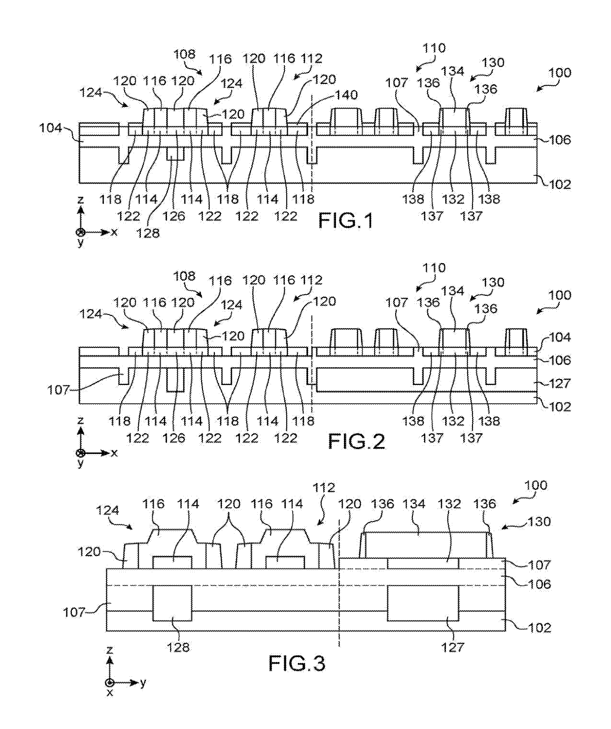
[0072]FIG. 1 shows a sectional view of a quantum device ;
second embodiment
[0073]FIGS. 2 and 3 show sectional views of a quantum device ;
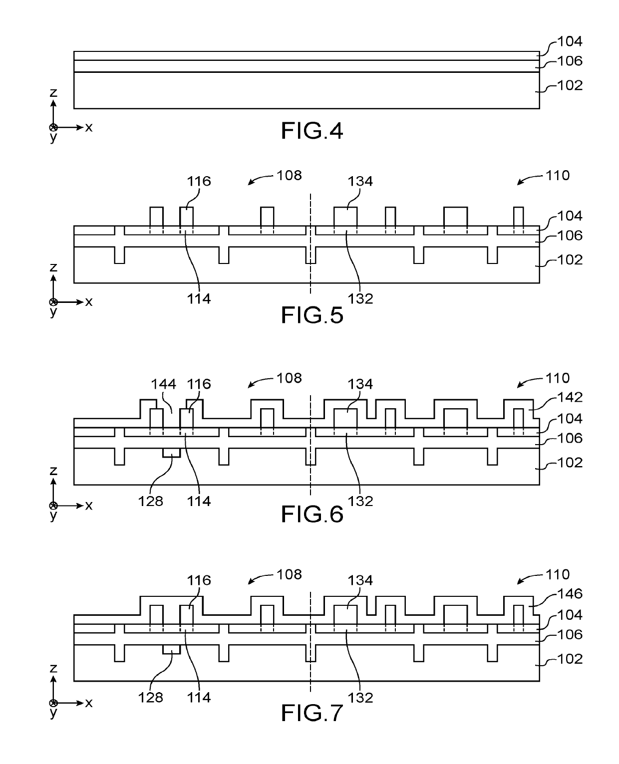
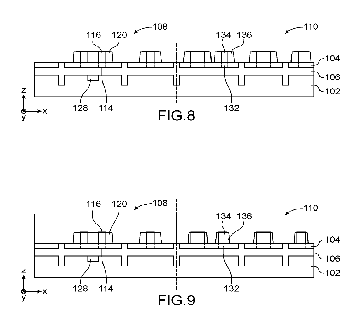
[0074]FIGS. 4 to 9 show the steps of a method for producing a quantum device according to the first embodiment.
[0075]Identical, similar or equivalent parts of the different figures described hereinafter bear the same reference numbers so as to facilitate the transition from one figure to another.
[0076]The different parts shown in the figures are not necessarily shown according to a uniform scale, to render the figures more legible.
[0077]The different options (alternative embodiments and embodiments) should be understood as not being mutually exclusive and may be combined with one another.
Login to View More PUM
 Abstract
Quantum device comprising:a quantum component forming a qubit, formed in an active layer of a substrate and comprising:a confinement region;charge carrier reservoirs;a first front gate covering the confinement region;first lateral spacers arranged around the first gate and covering access regions;an FET transistor formed in the active layer, comprising channel, source and drain regions formed in the active layer, a second front gate covering the channel region, and second lateral spacers arranged around the second front gate and covering source and drain extension regions;and wherein a width of the first lateral spacers is greater than that of the second lateral spacers.
Description
[0001]TECHNICAL FIELD AND PRIOR ART[0002]The invention relates to the field of quantum devices, spintronics, quantum data processing and quantum computing.[0003]A quantum device with one or a plurality of spin qubits, also known as “quantum bits” or “quantum dots”, makes it possible to manipulate the quantum state of this or these qubits. Such a quantum device operates at low temperature, generally a few hundred mK. The spin qubits may be made in semiconductor, advantageously silicon.[0004]A quantum device is controlled by control signals emitted by an electronic control circuit which is generally at a distance from the qubits and which is designed to operate at ambient temperature. This separation between the electronic control part and the part comprising the qubits is the source of multiple problems, particularly: management of the connections between these two parts, presence of parasitic passive elements, need to integrate attenuators and amplifiers close to the qubits.[0005]In...
Claims
Login to View More Application Information
Patent Timeline
 Patent Type & AuthorityApplications(United States)
IPC IPC(8): G06N10/00H01L29/76H01L29/66H01L21/762
CPCG06N10/00H01L21/76243H01L29/66439H01L29/7613H01L21/823468H01L21/84H01L27/088H01L27/1203H01L29/0653H01L29/08H01L29/66977H01L29/66984
InventorHUTIN, LOUISJEHL, XAVIERVINET, MAUD
OwnerCOMMISSARIAT A LENERGIE ATOMIQUE ET AUX ENERGIES ALTERNATIVES