
Vertical spin orbit torque devices

a torque device and spin orbit technology, applied in the field of magnetic random access memories, can solve the problems of large footprint of memory cells using so torque, waste of spin current, and inefficient switching of free layer torque, etc., and achieve the effects of improving torque, enhancing the interface of spin current, and improving the performance of magnetic devices using

Active Publication Date: 2019-09-05
SAMSUNG ELECTRONICS CO LTD
View PDF0 Cites 14 Cited by
  • Summary
  • Abstract
  • Description
  • Claims
  • Application Information

AI Technical Summary

Benefits of technology

The patent text describes a way to improve the performance of magnetic devices by using a specific method to write magnetic junctions. This method can enhance the interface for spin currents, make devices more scalable, reduce the number of selection devices needed, shorten switching time, optimize read and write operations, and reduce breakdown of a tunneling barrier in some aspects.

Problems solved by technology

In general, SO torque is not an efficient mechanism for switching the free layer.
Thus, this spin current may be wasted.
Memory cells using SO torque may have a large footprint because a three-terminal device may be used for write and read operations.
Perpendicular magnetic moments in the layers of the magnetic junction may also not be usable in some embodiments.
Thus, scalability may be limited.

Method used


Image

  • Vertical spin orbit torque devices
  • Vertical spin orbit torque devices
  • Vertical spin orbit torque devices

Examples


Embodiment Construction

[0026]The exemplary embodiments relate to magnetic junctions usable in magnetic devices, such as magnetic memories and / or logic devices, and the devices using such magnetic junctions. The magnetic memories may include magnetic random-access memories (MRAMs) and may be used in electronic devices employing nonvolatile memory. Such electronic devices include but are not limited to cellular phones, smart phones, tables, laptops and other portable and non-portable computing devices. The following description is presented to enable one of ordinary skill in the art to make and use the invention and is provided in the context of a patent application and its requirements. Various modifications to the exemplary embodiments and the generic principles and features described herein will be readily apparent. The exemplary embodiments are mainly described in terms of particular methods and systems provided in particular implementations. However, the methods and systems will operate effectively in ...


PUM

PropertyMeasurementUnit
nonzero angleaaaaaaaaaa
currentaaaaaaaaaa
magnetic statesaaaaaaaaaa

Abstract

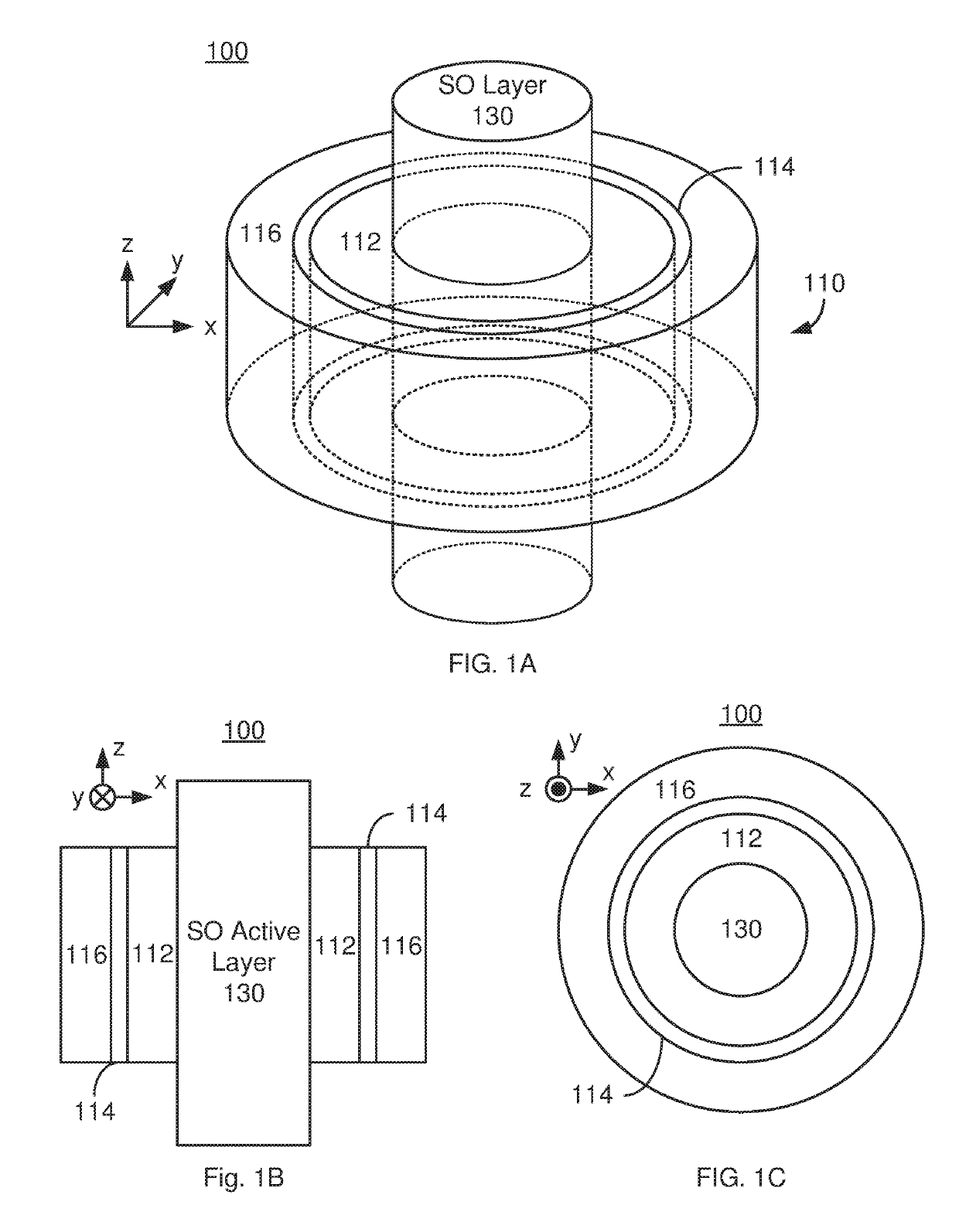
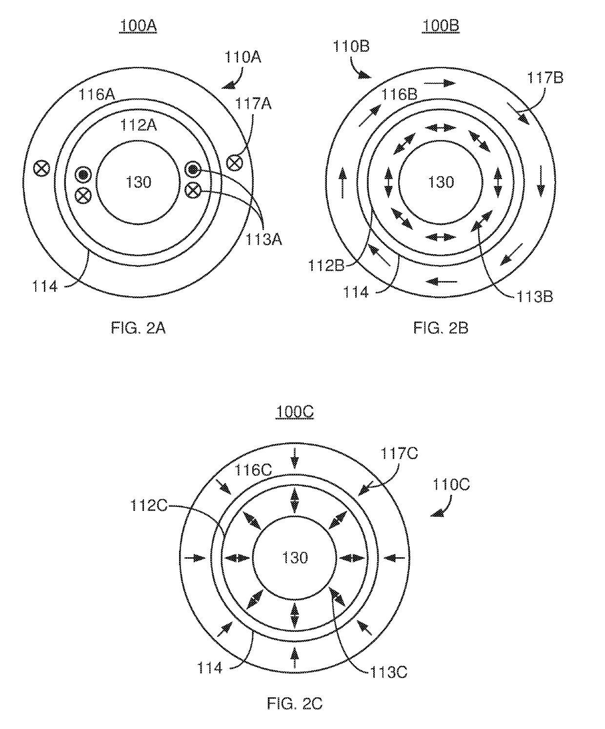
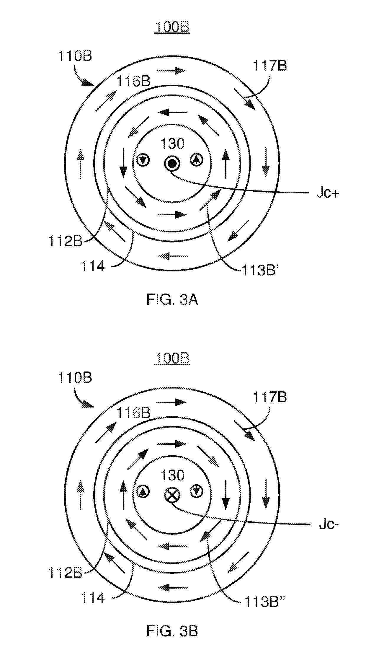
A magnetic device and method for programming the magnetic device are described. The magnetic device includes a plurality of magnetic junctions and at least one spin-orbit interaction (SO) active layer having a plurality of sides. The SO active layer(s) carry a current in direction(s) substantially perpendicular to the plurality of sides. Each of the magnetic junction(s) is adjacent to the sides and substantially surrounds a portion of the SO active layer. Each magnetic junction includes a free layer, a reference layer and a nonmagnetic spacer layer between the pinned and free layers. The SO active layer(s) exert a SO torque on the free layer due to the current passing through the SO active layer(s). The free layer is switchable between stable magnetic states. The free layer may be written using the current and, in some aspects, another current driven through the magnetic junction.

Description

CROSS-REFERENCE TO RELATED APPLICATIONS[0001]This application claims the benefit of provisional Patent Application Ser. No. 62 / 637,596, filed Mar. 2, 2018, entitled VERTICAL SPIN ORBIT TORQUE DEVICES INCLUDING MAGNETIC RANDOM ACCESS MEMORY, assigned to the assignee of the present application, and incorporated herein by reference.BACKGROUND OF THE INVENTION[0002]Magnetic memories, particularly magnetic random-access memories (MRAMs), have drawn increasing interest due to their potential for high read / write speed, excellent endurance, non-volatility and low power consumption during operation. An MRAM can store information utilizing magnetic materials as an information recording medium. Some magnetic memories write to the magnetic material using a current. One such magnetic memory programs magnetic junctions using spin-orbit interaction (SO) torque.[0003]SO torque-based memories, such as a SO torque magnetic random-access memory (SOT-MRAM), utilize conventional magnetic tunneling junct...

Claims


Application Information

Patent Timeline
Patent Type & Authority Applications(United States)
IPC IPC(8): H01L43/08H01L27/22H01L43/02G11C11/16H01F10/32H01L43/12H10N50/10H10N50/01H10N50/80
CPCH01L43/08H01L27/228H01L43/02G11C11/1675H01F10/329H01F10/3272G11C11/161H01F10/3286G11C11/1673H01L43/12H01F10/3254H10B61/22H10N50/80H10N50/10G11C11/1659G11C11/155H10N50/01H10N52/00
Inventor NIKITIN, VLADIMIRAPALKOV, DMYTRO
Owner SAMSUNG ELECTRONICS CO LTD
Learn More