
Manufacturing method for display panel, display panel and display device

a manufacturing method and display panel technology, applied in the field of touch display, can solve the problems of increasing the difficulty of addressing the problem of how to combine display technology and touch technology to make the light-emitting device thinner, and the increase of the demand for thin screens. , to achieve the effect of reducing the number of manufacturing steps, reducing the thickness of the display device, and avoiding the effect of touching the touch panel to the package structur

Inactive Publication Date: 2019-09-26
WUHAN CHINA STAR OPTOELECTRONICS SEMICON DISPLAY TECH CO LTD
View PDF2 Cites 4 Cited by
  • Summary
  • Abstract
  • Description
  • Claims
  • Application Information

AI Technical Summary

Benefits of technology

The present invention provides a manufacturing method for display panel, display panel, and display device that can reduce the thickness of the display panel and make the display device thinner. This is achieved by embedding touch electrodes in the display panel, which can serve as both a touch drive electrode and a touch sense electrode. This method avoids attaching a separate touch panel to the display, reducing the thickness of the display device and production cost.

Problems solved by technology

Therefore, in smart mobile displays, AMOLED display technology and touch technology need to be combined; in addition, the demands for thin screen are also increasing higher, therefore, how to combine the display technology with the touch technology to make the light-emitting device thinner has become an issue to be addressed.

Method used


Image

  • Manufacturing method for display panel, display panel and display device
  • Manufacturing method for display panel, display panel and display device
  • Manufacturing method for display panel, display panel and display device

Examples


Embodiment Construction

[0022]To further explain the technical means and effect of the present invention, the following refers to embodiments and drawings for detailed description. Apparently, the described embodiments are merely some embodiments of the present invention, instead of all embodiments. All other embodiments based on embodiments in the present invention and obtained by those skilled in the art without departing from the creative work of the present invention are within the scope of the present invention.

[0023]The terms “comprising” and “having” and any variations thereof appearing in the specification, claims, and drawings of the present application are intended to cover non-exclusive inclusion. For example, a process, method, system, product, or device that includes a series of steps or units is not limited to the listed steps or units, but optionally also includes steps or units not listed, or alternatively, other steps or units inherent to these processes, methods, products or equipment. In...


PUM


Abstract

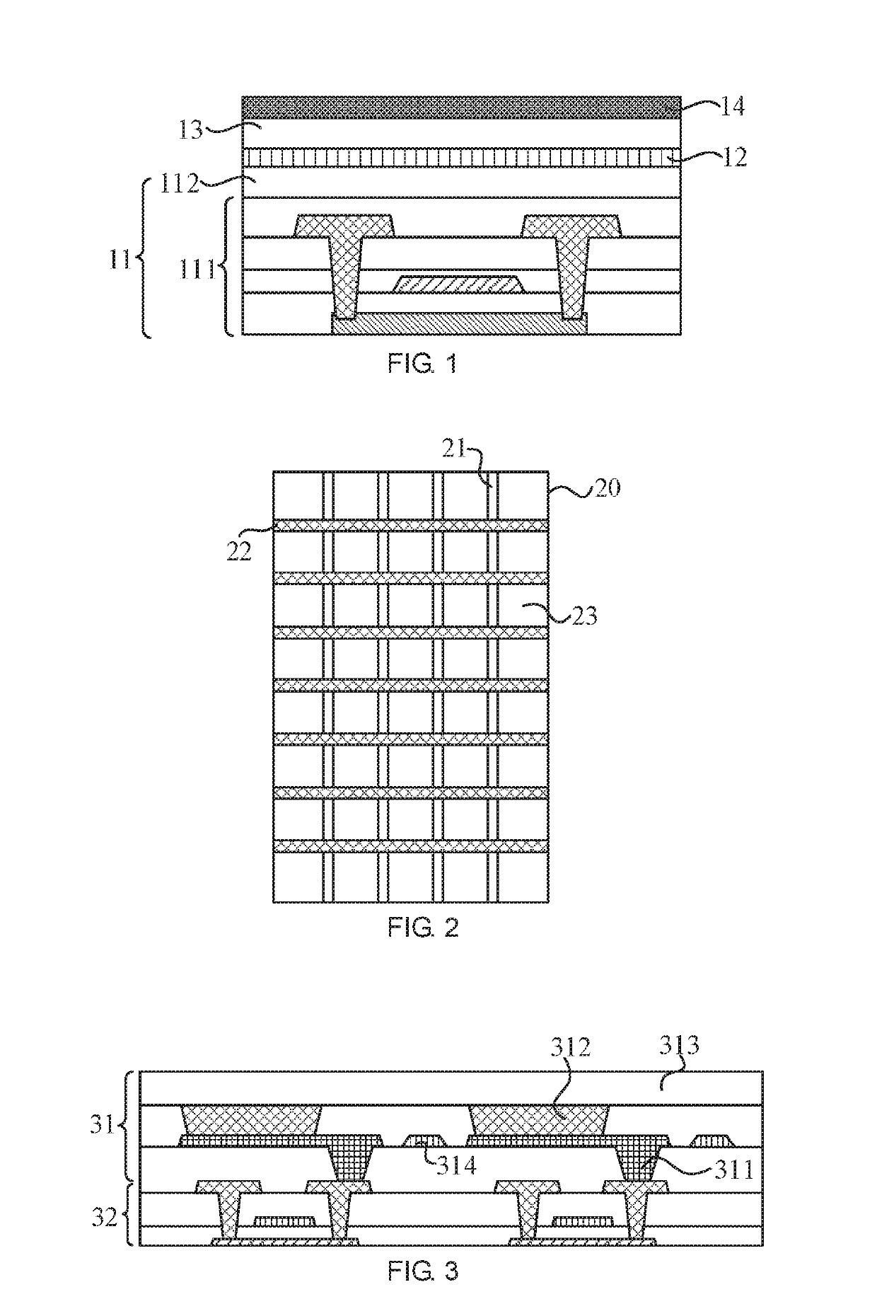
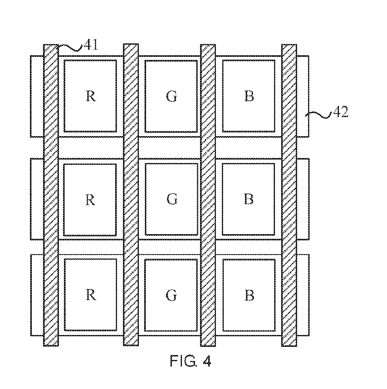
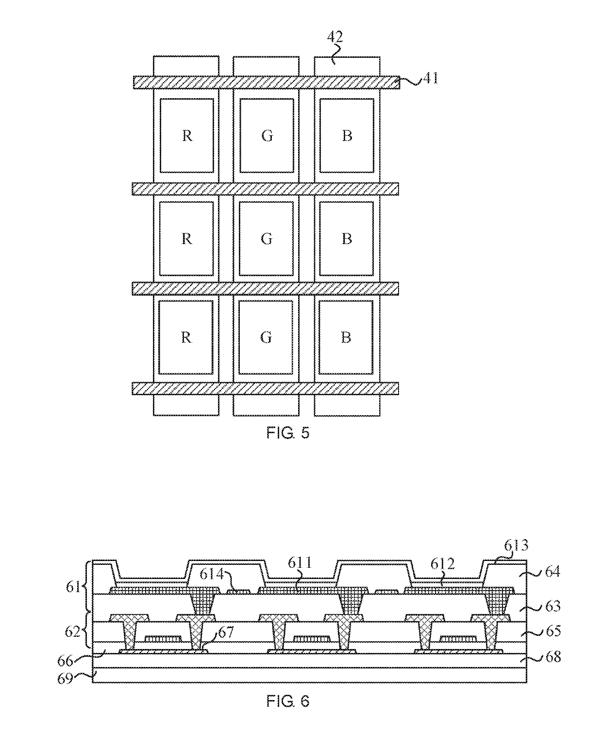
The invention provides a manufacturing method for display panel, display panel and display device. The display panel comprises a plurality of pixel units. Each pixel unit comprises a light-emitting element and a TFT, the light-emitting element comprises: an anode and a first touch electrode, disposed in a same layer, a light-emitting layer disposed on the anode and the first touch electrode, and a first electrode disposed on the light-emitting layer. The first electrode serves as a cathode of the display panel and a second touch electrode of the display panel in a time division manner. As such, the invention can reduce the thickness of the display panel and thickness of display device.

Description

BACKGROUND OF THE INVENTION1. Field of the Invention[0001]The present invention relates to the field of touch display and, in particular, to the field of manufacturing method for display panel, display panel and display device.2. The Related Arts[0002]Active matrix organic light-emitting diode (AMOLED) display provides the advantages of high response speed, power saving, applicability to portable devices, wide operating temperature range, higher contrast, and wider viewing angle. As such, AMOLED is expected to become the next generation of new flat panel display replacing liquid crystal display (LCD). As the flexible AMOLED has the advantages of being light and thin, bendable or foldable, and the shape of the flexible AMOLED can be arbitrarily changed, it has received increasing attention from the market.[0003]In general, smart mobile displays need to integrate touch screen technology in order to facilitate user for use and operation. Therefore, in smart mobile displays, AMOLED disp...

Claims


Application Information

Patent Timeline
IPC IPC(8): G06F3/041
CPCG06F3/0412G06F2203/04103G06F3/0446G06F3/0445H10K59/40
Inventor ZENG, MIAN
Owner WUHAN CHINA STAR OPTOELECTRONICS SEMICON DISPLAY TECH CO LTD
Learn More