TFT pixel threshold voltage compensation circuit with data voltage applied at light-emitting device

a compensation circuit and data voltage technology, applied in the direction of instruments, static indicating devices, etc., can solve the problems of memory effects from previous frame data, affecting the true black state, and pixels in the display may not exhibit uniform brightness for a given vdat value, so as to reduce or eliminate memory effects

Active Publication Date: 2019-09-26
SHARP KK
View PDF6 Cites 6 Cited by
  • Summary
  • Abstract
  • Description
  • Claims
  • Application Information

AI Technical Summary

Benefits of technology

[0009]The present invention relates to pixel circuits that are capable of compensating the threshold voltage variations of the drive transistor with fewer transistors than in conventional configurations, with additionally removing the possible memory effects associated with the OLED device and drive transistor from the previous frame. The described circuit configurations, therefore, improve the capability of a pixel to emit very little or no light and therefore have a true black state.
[0014]ii) Below the voltage which would be applied to the OLED anode during the subsequent emission phase, and corresponding to the current (or luminance) of the OLED which is designated by the VDAT value.As a consequence, there will be no light emission from the OLED during the programming phase, or the luminance from the OLED during the programming phase is less than the designed luminance during the subsequent emission phase. Therefore, the minimum luminance from the pixel is low, and the true darkness will be improved.
[0015]When VDAT is applied at the anode of the OLED during the programming phase, the voltage at the terminal of the OLED is reset or initialized to VDAT. Memory effects associated with the OLED, whereby the voltage at the anode of the OLED from the previous frame affects the circuit operation during the present frame, are therefore reduced or eliminated. In other embodiments, the VDAT may be applied to the cathode of the OLED during the programming phase, with comparable effect to reduce or eliminate memory effects.
[0016]In addition, a voltage at the gate of the drive transistor is reset during an initialization phase. In this manner, memory effects associated with the drive transistor also are reduced or eliminated.
[0017]Embodiments of the present invention have advantages over conventional configurations. Such advantages include, for example, providing effective threshold voltage compensation, reduction or elimination of memory effects, true black improvements and efficient data programming. Exemplary embodiments utilize only four transistors and as few as one capacitor for the above functions.

Problems solved by technology

Therefore, pixels in a display may not exhibit uniform brightness for a given VDAT value.
A first problem with this is that it may affect the true black state.
A second problem is memory effects from the previous frame data.
If the programmed current is a low current, it could take a significant time to refresh the anode to the programmed value.
There are significant drawbacks with such configuration and method.
This may cause an instance of high luminance light, which would prevent a pixel from ever having a true black state.
Other approaches to address the above problems have proven deficient.
This approach, however, could cause a leakage current during the programming phase, which may affect the blackness in low current operations.
This configuration, however, increases the transistor number to seven in the circuit, which will lower the yield and be difficult to implement in high resolution applications requiring a small geometry.
U.S. Pat. No. 9,337,439B2 (Kwon, issued May 10, 2016) describes a scheme to improve the blackness by using previous data, but the number of transistors is still high and the residual voltage at the anode of the OLED could still cause some light leakage in low current.

Method used


Image

  • TFT pixel threshold voltage compensation circuit with data voltage applied at light-emitting device
  • TFT pixel threshold voltage compensation circuit with data voltage applied at light-emitting device
  • TFT pixel threshold voltage compensation circuit with data voltage applied at light-emitting device

Examples


Embodiment Construction

[0032]Embodiments of the present invention will now be described with reference to the drawings, wherein like reference numerals are used to refer to like elements throughout. It will be understood that the figures are not necessarily to scale.

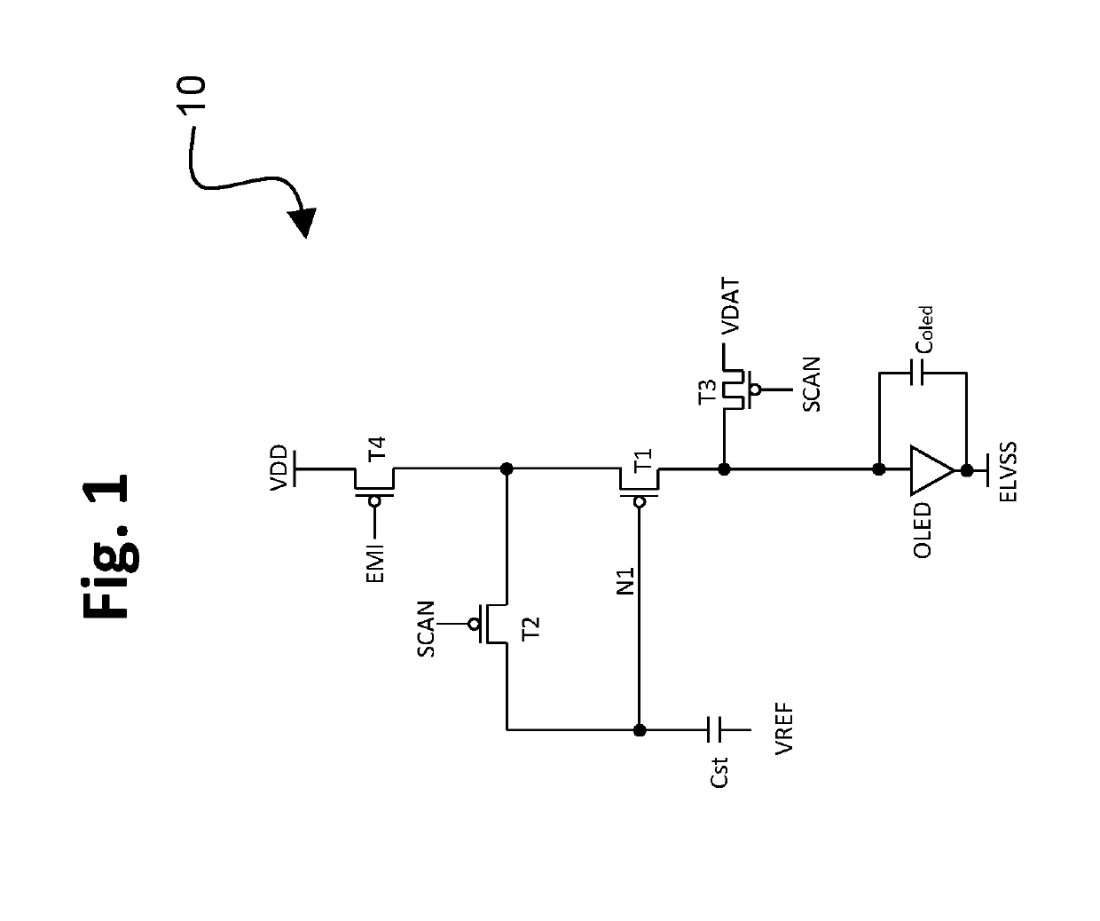
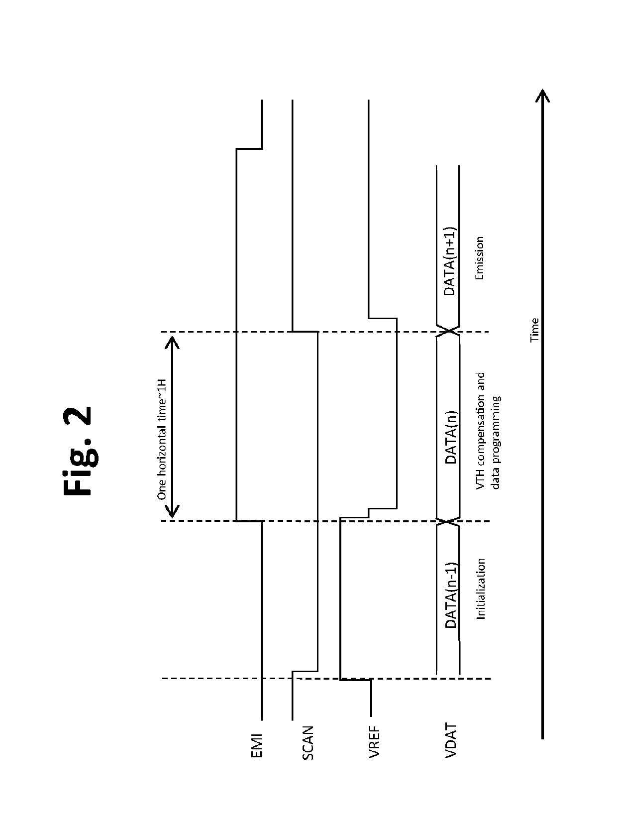
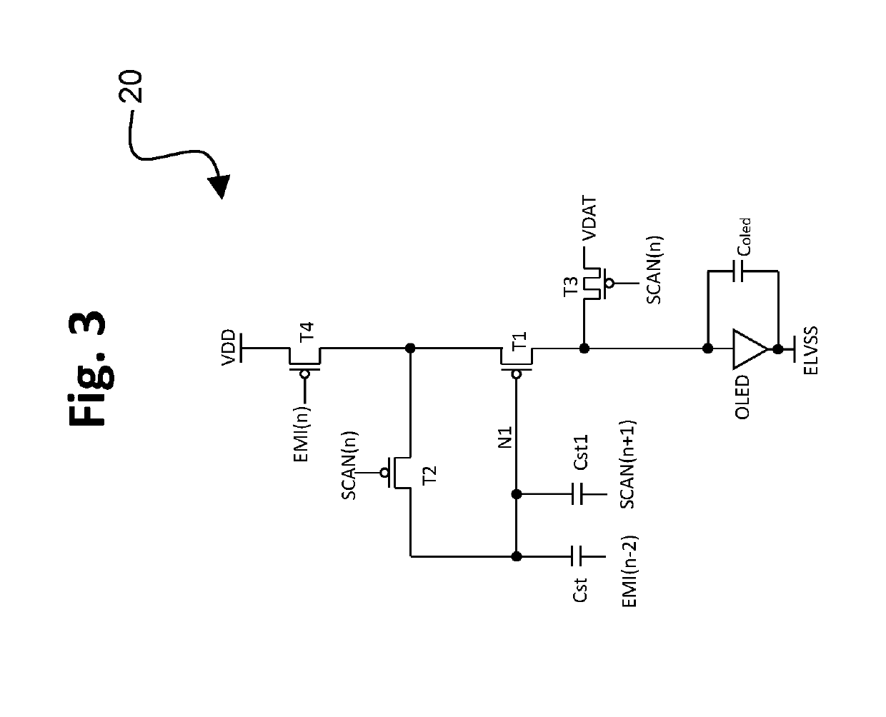
[0033]FIG. 1 is a drawing depicting a first circuit configuration 10 in accordance with embodiments of the present invention, and FIG. 2 is a timing diagram associated with the circuit configuration of FIG. 1. In this example, the circuit 10 is configured as a TFT circuit that includes multiple p-type transistors T1-T4 and a single storage capacitor Cst. The circuit elements drive a light-emitting device, such as for example an OLED. The light-emitting device (OLED) has an associated internal capacitance, which is represented in the circuit diagram as Coled. In addition, although the embodiments are described principally in connection with an OLED as the light-emitting device, comparable principles may be used with display technologies that em...


PUM


Abstract

A pixel circuit for a display device includes a drive transistor configured to control an amount of current to a light-emitting device depending upon a voltage applied to a gate of the drive transistor; a second transistor connected to the gate of the drive transistor and a second terminal of the drive transistor, such that when the second transistor is in an on state the drive transistor becomes diode-connected such that the gate and the second terminal of the drive transistor are connected through the second transistor; a light-emitting device that is connected at a first node to a third terminal of the drive transistor and at a second node to a first voltage supply; a third transistor connected to the first node of the light-emitting device, which connects a data voltage to the first node of the light-emitting device; a fourth transistor that is connected between the second terminal of the drive transistor and a second voltage supply; and at least one capacitor having a first plate that is connected to the gate of the drive transistor and a second plate that is connectable to a reference signal. The pixel circuit is operable during a phase preceding the emission phase including applying a data voltage to the first node of the light-emitting device and the third terminal of the drive transistor, the data voltage being set so that a voltage across the light-emitting device is lower than a threshold voltage of the light emitting device.

Description

TECHNICAL FIELD[0001]The present invention relates to design and operation of electronic circuits for delivering electrical current to an element in a display device, such as for example to an organic light-emitting diode (OLED) in the pixel of an active matrix OLED (AMOLED) display device.BACKGROUND ART[0002]Organic light-emitting diodes (OLED) generate light by re-combination of electrons and holes, and emit light when a bias is applied between the anode and cathode such that an electrical current passes between them. The brightness of the light is related to the amount of the current. If there is no current, there will be no light emission, so OLED technology is a type of technology capable of absolute blacks and achieving almost “infinite” contrast ratio between pixels when used in display applications.[0003]Several approaches are taught in the prior art for pixel thin film transistor (TFT) circuits to deliver current to an element of a display device, such as for example an org...

Claims


Application Information

Patent Timeline
Patent Type & Authority Applications(United States)
IPC IPC(8): G09G3/3291G09G3/3266
CPCG09G3/3291G09G2310/066G09G2300/0852G09G2320/0238G09G3/3266G09G3/3233G09G3/32G09G2320/0233G09G2320/043G09G2300/0819G09G2300/0861G09G2310/0251G09G2310/0262
Inventor LU, TONGBROWNLOW, MICHAEL JAMESSMEETON, TIM MICHAELUEDA, NAOKI
Owner SHARP KK
Why Eureka
Try Eureka