Hot spot defect detecting method and hot spot defect detecting system

a defect detection and defect technology, applied in the field of hot spot defect detection methods and hot spot defect detection systems, can solve the problems of optical inspection tools showing more and more gaps in detecting various types of defects, wafer noise limitation of existing optical inspection tools, and defect signals becoming even weaker than wafer nois

Active Publication Date: 2019-10-17
TAIWAN SEMICON MFG CO LTD
View PDF5 Cites 13 Cited by
  • Summary
  • Abstract
  • Description
  • Claims
  • Application Information

AI Technical Summary

Problems solved by technology

The sensitivity of existing optical inspection tool is limited by wafer noise.
Since defect size continues to decrease along with advancement of process, the defect si

Method used


Image

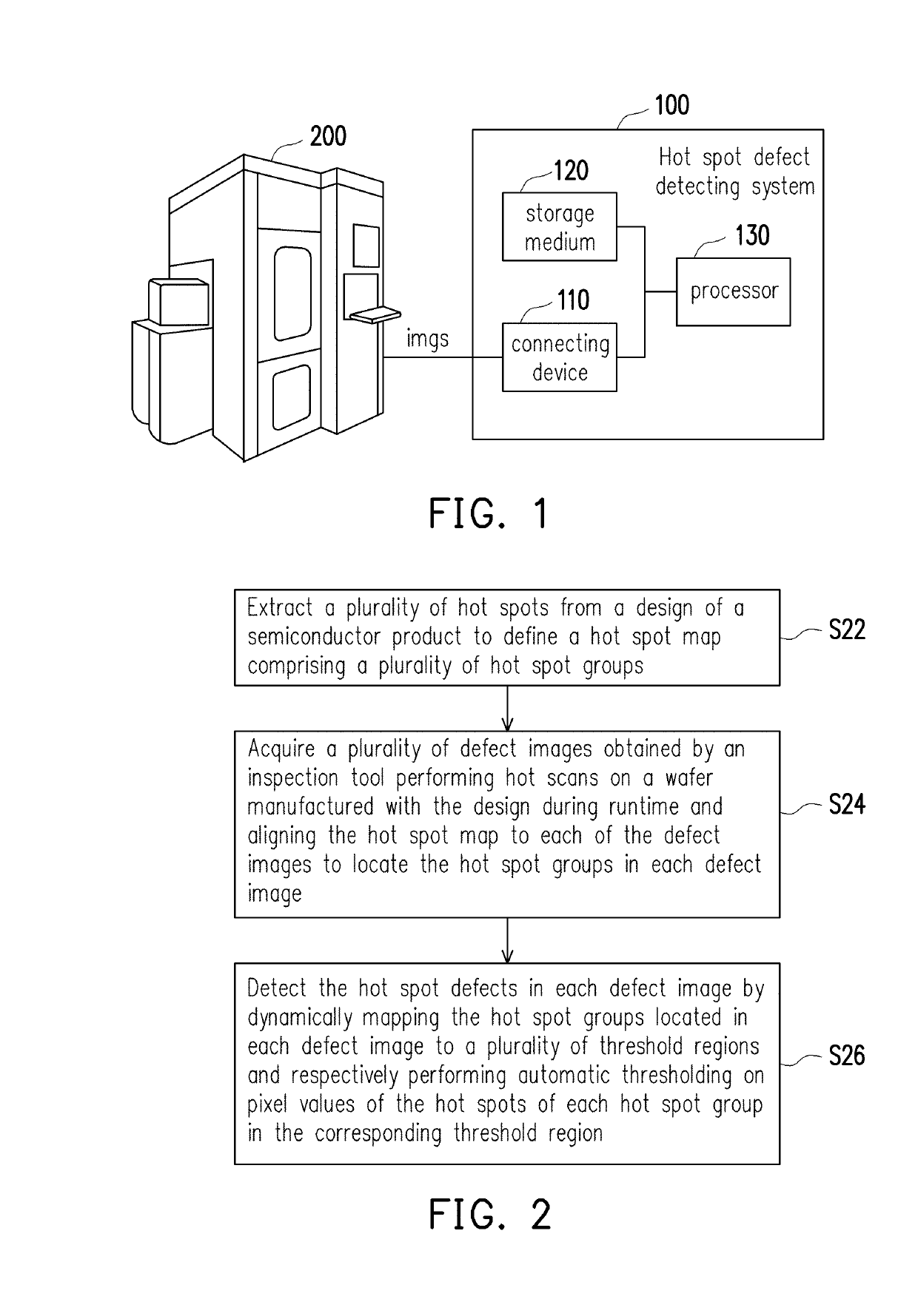
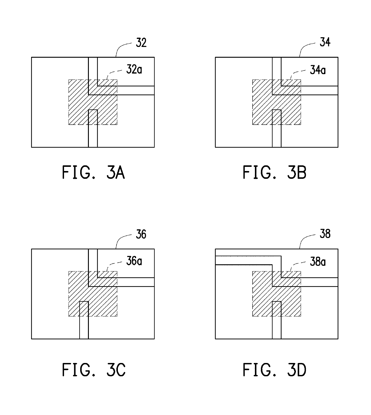
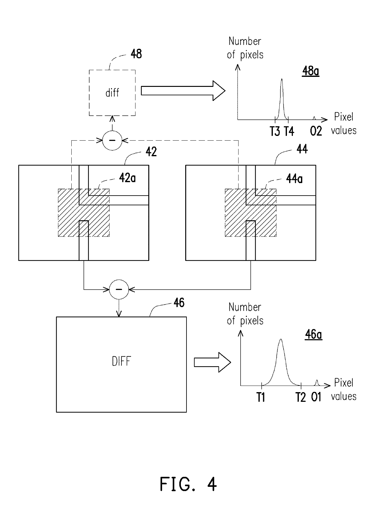
  • Hot spot defect detecting method and hot spot defect detecting system
  • Hot spot defect detecting method and hot spot defect detecting system
  • Hot spot defect detecting method and hot spot defect detecting system

Examples


Embodiment Construction

[0014]The following disclosure provides many different embodiments, or examples, for implementing different features of the provided subject matter. Specific examples of components and arrangements are described below to simplify the present disclosure. These are, of course, merely examples and are not intended to be limiting. For example, the formation of a first feature over or on a second feature in the description that follows may include embodiments in which the first and second features are formed in direct contact, and may also include embodiments in which additional features may be formed between the first and second features, such that the first and second features may not be in direct contact. In addition, the present disclosure may repeat reference numerals and / or letters in the various examples. This repetition is for the purpose of simplicity and clarity and does not in itself dictate a relationship between the various embodiments and / or configurations discussed.

[0015]F...


PUM


Abstract

A hot spot defect detecting method and a hot spot defect detecting system are provided. In the method, hot spots are extracted from a design of a semiconductor product to define a hot spot map comprising hot spot groups, wherein local patterns in a same context of the design yielding a same image content are defined as a same hot spot group. During runtime, defect images obtained by an inspection tool performing hot scans on a wafer manufactured with the design are acquired and the hot spot map is aligned to each defect image to locate the hot spot groups. The hot spot defects in each defect image are detected by dynamically mapping the hot spot groups located in each defect image to a plurality of threshold regions and respectively performing automatic thresholding on pixel values of the hot spots of each hot spot group in the corresponding threshold region.

Description

CROSS REFERENCE TO RELATED APPLICATION[0001]This application claims the priority benefit of U.S. provisional application Ser. No. 62 / 656,997, filed on Apr. 13, 2018. The entirety of the above-mentioned patent application is hereby incorporated by reference herein and made a part of specification.BACKGROUND OF THE INVENTION[0002]In the manufacturing processes of modern semiconductor devices, various materials and machines are manipulated to create a final product. Manufacturers have dedicated to reduce particulate contamination during processing so as to improve product yield. Due to the increasing complexity of semiconductor devices and the development of ultra-small transistors, the need for defect detection and control is further emphasized.[0003]The inspection on the semi-manufactured product is frequently performed during manufacturing by using optical inspection tool in order to timely find the defects. The sensitivity of existing optical inspection tool is limited by wafer noi...

Claims


Application Information

Patent Timeline
IPC IPC(8): G06T7/00
CPCG06T2207/20081G06T2207/30148G06T7/0006G01N21/8851G06T7/0004G01N2021/8887G01N2021/8861G01N2021/8877G06T2207/10004G06T7/001G06T2207/30141G01N21/9505G01N2021/8854G06N3/04G06N3/08G06T2207/20084G06T2207/30168
Inventor CHEN, CHIEN-HUEISU, PEI-CHAOCHEN, XIAOMENGCHANG, CHAN-MINGCHEN, SHIH-YUNGCHUNG, HUNG-YICHEN, KUANG-SHINGLEE, LI-JOULIN, YUNG-CHENGWU, WEI-CHENWANG, SHIH-CHANGLIN, CHIEN-AN
Owner TAIWAN SEMICON MFG CO LTD
Why Eureka
Try Eureka