ESD protection circuit, related display panel with protection against ESD, and ESD protection structure

a technology of esd protection circuit and display panel, which is applied in the direction of semiconductor devices, diodes, electrical apparatus, etc., can solve the problems of display panel damage, inability to reverse damage to transistors, and complicated manufacturing processes

Inactive Publication Date: 2019-10-24
AU OPTRONICS CORP
View PDF0 Cites 8 Cited by
  • Summary
  • Abstract
  • Description
  • Claims
  • Application Information

AI Technical Summary

Benefits of technology

[0005]The disclosure provides a display panel with protection against ESD. The display panel including an active area, a gate driver, and a plurality of ESD protection circuits. The active area includes a plurality of pixels. The gate driver is configured to drive the plurality of pixels. The plurality of ESD protection circuits is disposed in the active area or a peripheral area surrounding the active area, and configured to provide a plurality of control signals to the gate driver. Each of the plurality of ESD protection circuits includes a first diode element, a second diode element, a first clamping circuit, a second clamping circuit, and a protection circuit. The first diode element is coupled between a first power node and an input node, and the input node is configured to receive one of the plurality of control signals. The second diode element is coupled between a second power node and the input node. The first clamping circuit is coupled between the first power node and the second power node. The second clamping circuit is coupled between the second power node and the input node. The protection circuit is coupled between the first power node and the second power node, and configured to transmit a current corresponding to an ESD event to a grounded capacitor.

Problems solved by technology

The breakthrough effect, however, brings irreversible damage to the transistor.
Therefore, the conventional ESD protection circuit provides very limited times of protection, which results that the display panel may still be damaged during the numerous steps of the cell and module processes.
With respect to micro-LED displays, the mass transfer technology renders the manufacturing process more complicated, and thus the conventional ESD protection circuit is even more unsuitable for the micro-LED displays.

Method used


Image

  • ESD protection circuit, related display panel with protection against ESD, and ESD protection structure
  • ESD protection circuit, related display panel with protection against ESD, and ESD protection structure
  • ESD protection circuit, related display panel with protection against ESD, and ESD protection structure

Examples


Embodiment Construction

[0017]Reference will now be made in detail to the present embodiments of the disclosure, examples of which are illustrated in the accompanying drawings. Wherever possible, the same reference numbers are used in the drawings and the description to refer to the same or like parts.

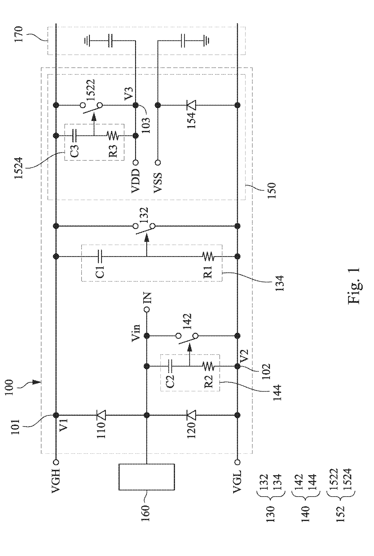
[0018]FIG. 1 is a functional block diagram of an ESD protection circuit 100 according to one embodiment of the present disclosure. The ESD protection circuit 100 comprises a first diode element 110, a second diode element 120, a first clamping circuit 130, a second clamping circuit 140, and a protection circuit 150. An input node IN of the ESD protection circuit 100 is coupled with an internal circuit 160, protected by the ESD protection circuit 100, and the input node IN is configured to receive signals that the internal circuit 160 needs.

[0019]A first node of the first diode element 110 (e.g., an anode) is coupled with the input node IN. A second node of the first diode element 110 (e.g., an cathode) is cou...


PUM


Abstract

An ESD protection circuit includes a first diode element, a second diode element, a first clamping circuit, a second clamping circuit, and a protection circuit. The first diode element is coupled between a first power node and an input node, wherein the input node is coupled with an internal circuit. The second diode element is coupled between a second power node and the input node. The first clamping circuit is coupled between the first power node and the second power node. The second clamping circuit is coupled between the second power node and the input node. The protection circuit is coupled between the first power node and the second power node, and configured to transmit a current corresponding to an ESD event to a grounded capacitor.

Description

CROSS-REFERENCE TO RELATED APPLICATION[0001]This application claims priority to U.S. Provisional Application Ser. No. 62 / 659,662, filed Apr. 18, 2018, which is herein incorporated by reference in its entirety.BACKGROUNDField of Invention[0002]The present disclosure relates to an ESD protection circuit, a display panel with protection against ESD, and an ESD protection structure. More particularly, the present disclosure relates to an ESD protection circuit including a clamping circuit including a switch and a sensing circuit.Description of Related Art[0003]The display panel manufacturing process consists of the array process, the cell process, and the module process. Electrostatic discharge (ESD) protection circuits are fabricated on the glass substrate during the array process to prevent pixels and peripheral driving circuits from damaged by the ESD event in the following processes. A clamping circuit of the conventional ESD protection circuit provides a discharging path for a curr...

Claims


Application Information

Patent Timeline
Patent Type & Authority Applications(United States)
IPC IPC(8): H02H9/04
CPCH02H9/046H01L27/0207H01L27/0255H01L27/0288H01L27/0296H02H9/02H01L2224/18
Inventor XI, PENG-BO
Owner AU OPTRONICS CORP
Why Eureka
Try Eureka