Stress sensor

a stress sensor and sensor technology, applied in the field of stress sensors, can solve the problem of limited detection direction of stress, and achieve the effect of high magnetoresistance change rate and the possibility of manufacturing of highly sensitive sensors

Active Publication Date: 2019-11-28
MURATA MFG CO LTD +1
View PDF0 Cites 0 Cited by
  • Summary
  • Abstract
  • Description
  • Claims
  • Application Information

AI Technical Summary

Benefits of technology

[0052]Thus, even in the arrangement of the electrodes 5a, 5b illustrated in FIG. 5, the same or substantially the same advantageous effects as those of the first preferred embodiment and the second preferred embodiment are able to be achieved. Note that, when the size of the element in the in-plane direction approximates the total film thickness (about 10 nm to about 300 nm, for example) of the metal layers, the arrangement of the electrodes 5a, 5b illustrated in FIG. 1 is likely to generate an electric current density distribution in a direction perpendicular or substantially perpendicular to the film surface of the stress detection layer 3, whereas in the arrangement of the electrodes 5a, 5b illustrated in FIG. 5, the electric current flows evenly.
[0053]In a fourth preferred embodiment of the present invention, a description of the matters common to the first preferred embodiment will be omitted, and only different points will be described.
[0054]FIG. 6 is a schematic cross-sectional view of a stress sensor according to the fourth preferred embodiment. As illustrated in FIG. 6, in the fourth preferred embodiment, an electrode 5a is provided on the protective layer 4, a portion of the base layer 2 is exposed, and an electrode 5b is provided on the exposed base layer 2. The fourth preferred embodiment is the same or substantially the same as the first and second preferred embodiments except for the arrangement of the electrodes 5a, 5b and that an insulator may be used as a non-magnetic layer 30. The non-magnetic layer 30 may be defined by an insulator, for example, using silicon oxide, silicon nitride, aluminum oxide, or magnesium oxide. It is preferable that the thickness of the non-magnetic layer 30 defined by the insulator should be thin enough to allow a tunnel electric current to flow, i.e., it is preferable to be set to about 5 nm or less, for example.
[0055]The arrangement of the electrodes 5a, 5b illustrated in FIG. 6 may cause the electric current to flow perpendicularly or substantially perpendicularly to the stress detection layer 3. Even in the arrangement of the electrodes 5a, 5b illustrated in FIG. 6, the above-described giant magnetoresistance effect is able to be detected because the electric current eventually flows through the entire thickness of the stress detection layer 3 when a voltage is applied between the electrode 5a and the electrode 5b. Further, when the arrangement illustrated in FIG. 6 includes the insulator for the non-magnetic layer 30, the arrangement of the electrodes 5a, 5b is able to detect a tunnel magnetoresistance effect in which the relative angle of magnetization is reflected in the resistance as in the giant magnetoresistance effect.
[0056]As described above, even in the arrangement of the electrodes 5a, 5b illustrated in FIG. 6, the same or substantially the same advantageous effects as those of the first preferred embodiment and the second preferred embodiment are able to be achieved. Note that the arrangement of the electrodes 5a, 5b illustrated in FIG. 6 may obtain a particularly high magnetoresistance change rate compared with those of the first preferred embodiment and the second preferred embodiment, and thus a highly sensitive sensor is able to be manufactured.
[0057]The present invention will be described further specifically with reference to examples of preferred embodiments of the present invention, but the present invention is not limited to these examples.

Problems solved by technology

However, although such a conventional stress sensor is able to detect the magnitude of a stress by the single element, there is a problem that a detectable direction of the stress is limited.

Method used


Image

  • Stress sensor
  • Stress sensor
  • Stress sensor

Examples


first preferred embodiment

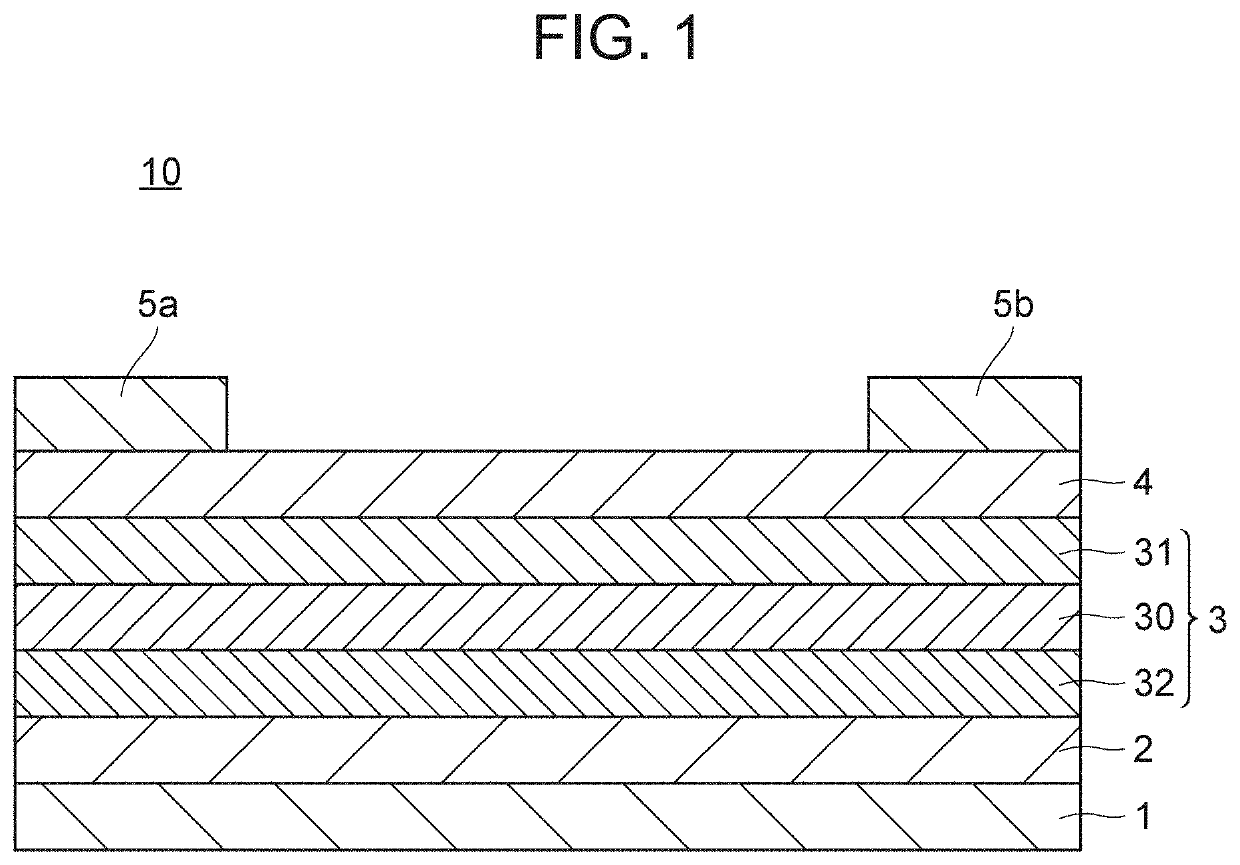
[0024]FIG. 1 is a cross-sectional view of a stress sensor according to a first preferred embodiment of the present invention.

[0025]As illustrated in FIG. 1, a stress sensor 10 includes a substrate 1, a base layer 2 on the substrate 1, a stress detection layer 3 on the base layer 2, a protective layer 4 on the stress detection layer 3, and electrodes 5a, 5b on the protective layer 4.

[0026]The substrate 1 is preferably a resin substrate, and use of a flexible substrate having flexibility and elasticity may be applied to a sensor to sense the movement of a human body, and the like. As such a flexible substrate, for example, a substrate made of polyester, polycarbonate, or polyimide is preferably used.

[0027]The base layer 2 determines the crystal orientation of the stress detection layer 3, and improves the adhesion of magnetic layers in the stress detection layer 3 to the substrate 1, which may be any non-magnetic body. For example, the base layer 2 is preferably made of Pt, Cu, Ta, Au...

second preferred embodiment

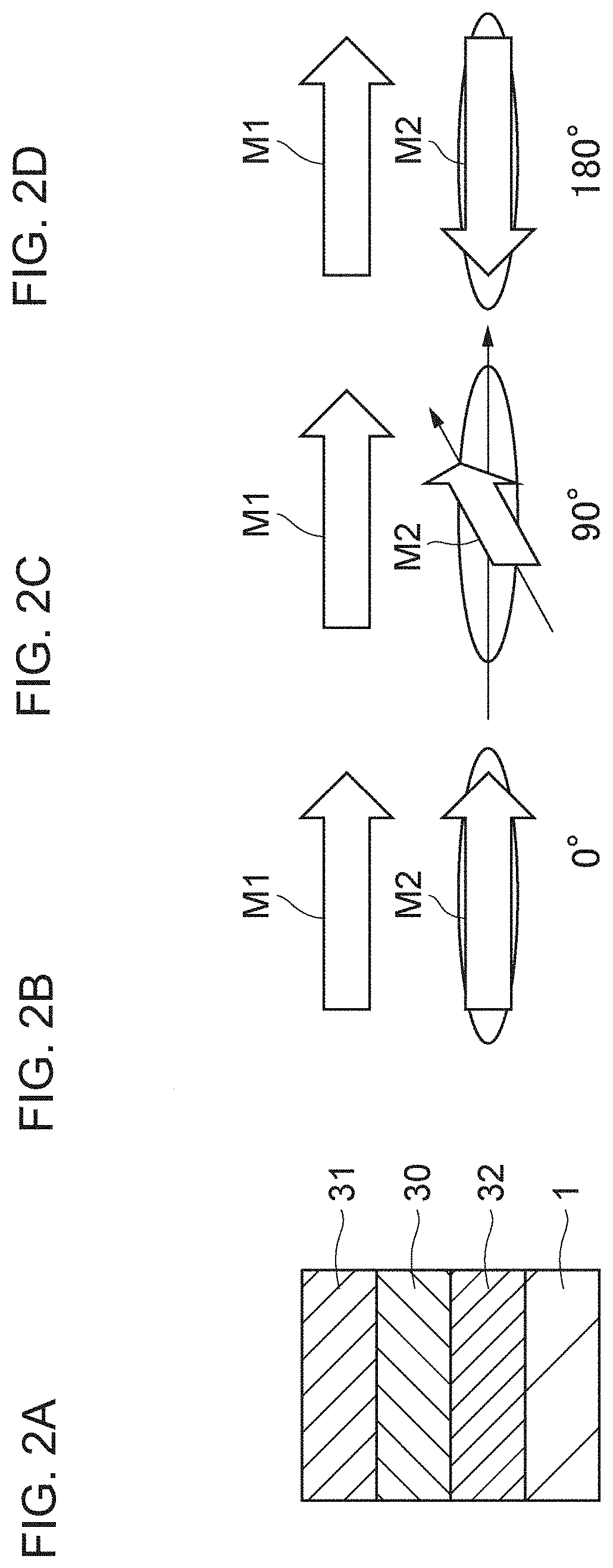
[0043]In a second preferred embodiment of the present invention, a description of the matters common to the first preferred embodiment will be omitted, and only different points will be described. The cross-sectional view of the stress sensor according to the second preferred embodiment is as illustrated in FIG. 1.

[0044]In the second preferred embodiment, either one of the first magnetic layer 31 and the second magnetic layer 32 has a positive magnetoelastic coupling constant, and the other one has a negative magnetoelastic coupling constant. For example, the magnetoelastic coupling constant of the first magnetic layer 31 is preferably negative, and the magnetoelastic coupling constant of the second magnetic layer 32 is preferably positive. In other words, when a stress (strain) acts on the stress sensor 10, the magnetization direction of the first magnetic layer 31(B32 (B>0) is turned to be parallel or substantially parallel to the strain direction. It is preferable that the absolu...

third preferred embodiment

[0049]In a third preferred embodiment of the present invention, a description of the matters common to the first preferred embodiment will be omitted, and only different points will be described.

[0050]FIG. 5 is a schematic cross-sectional view of a stress sensor according to the third preferred embodiment. As illustrated in FIG. 5, electrodes 5a, 5b are provided on the sides of the stress detection layer 3 in the third preferred embodiment. The structure is the same or substantially the same as that in the first and second preferred embodiments, except for the arrangement of the electrodes 5a, 5b and that an insulator may be used as the protective layer 4. When the insulator is used as the protective layer 4, for example, silicon oxide, silicon nitride, aluminum oxide, or magnesium oxide may preferably be used.

[0051]The arrangement of the electrodes 5a, 5b illustrated in FIG. 5 may also detect the above-described giant magnetoresistance effect because an electric current eventually ...


PUM

PropertyMeasurementUnit
thicknessaaaaaaaaaa
thicknessaaaaaaaaaa
thicknessaaaaaaaaaa

Abstract

A stress sensor includes a stress detection layer including a laminated body including a first magnetic layer, a first non-magnetic layer, and a second magnetic layer that are laminated, wherein the first magnetic layer and the second magnetic layer have mutually different magnetoelastic coupling constants, such that a stress is detected by an electrical resistance dependent on a relative angle of magnetization between the first magnetic layer and the second magnetic layer varying depending on the stress externally applied.

Description

CROSS REFERENCE TO RELATED APPLICATIONS[0001]This application claims the benefit of priority to Japanese Patent Application No. 2017-029314 filed on Feb. 20, 2017 and is a Continuation Application of PCT Application No. PCT / JP2018 / 004853 filed on Feb. 13, 2018. The entire contents of each application are hereby incorporated herein by reference.BACKGROUND OF THE INVENTION1. Field of the Invention[0002]The present invention relates to a stress sensor.2. Description of the Related Art[0003]As a conventional stress sensor, for example, there is known a method of using a resistor arranged to extend in a fixed direction as a sensor segment to detect a stress from a change in resistance value when this resistor is deformed by the stress in the longitudinal direction thereof (for example, see Japanese Patent Application Laid-Open No. 2007-333408).[0004]Japanese Patent Application Laid-Open No. 2007-333408 discloses a stress sensor as an example of a stress sensor using the above method, whi...

Claims


Application Information

Patent Timeline
Patent Type & Authority Applications(United States)
IPC IPC(8): G01L1/12H01F10/32
CPCG01L1/12H01F10/325H01F10/3259H01F10/3286G01R33/093G01R33/091H01F10/28
Inventor CHIBA, DAICHIANDO, AKIRA
Owner MURATA MFG CO LTD
Why Eureka
Try Eureka