Epidermal virtual reality devices
- Summary
- Abstract
- Description
- Claims
- Application Information
AI Technical Summary
Benefits of technology
Problems solved by technology
Method used
Image
Examples
example 1
Actuator-Containing Devices
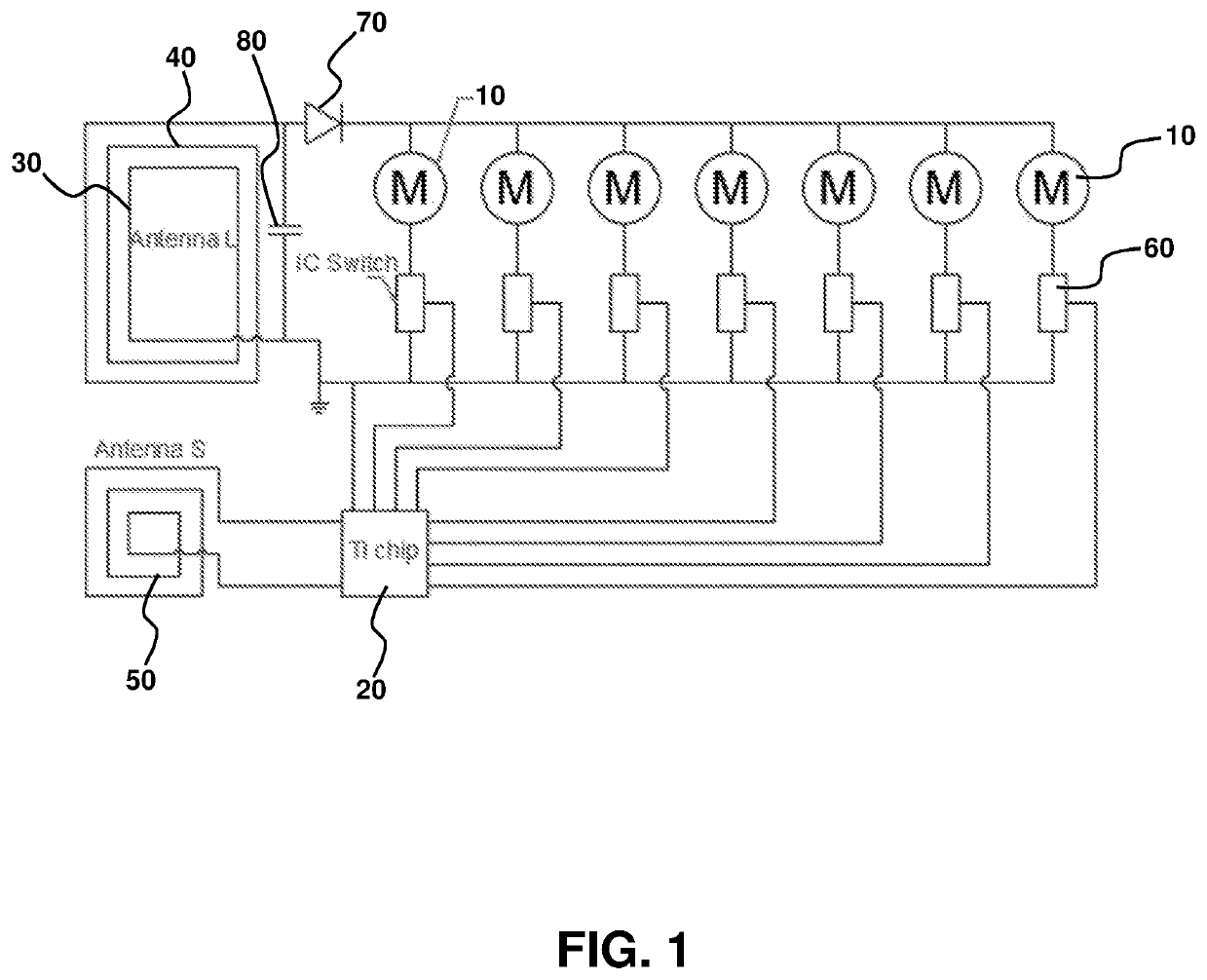
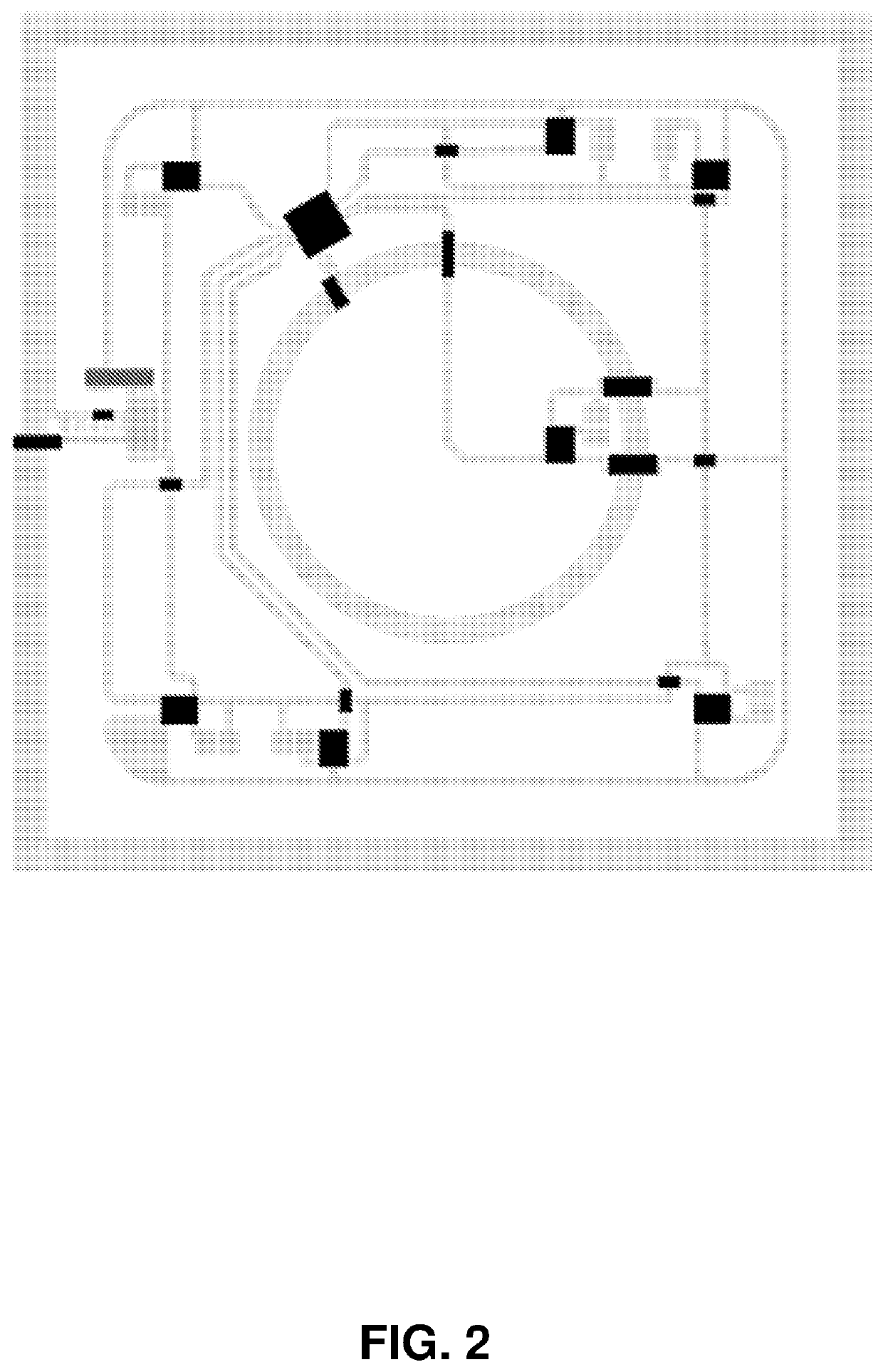
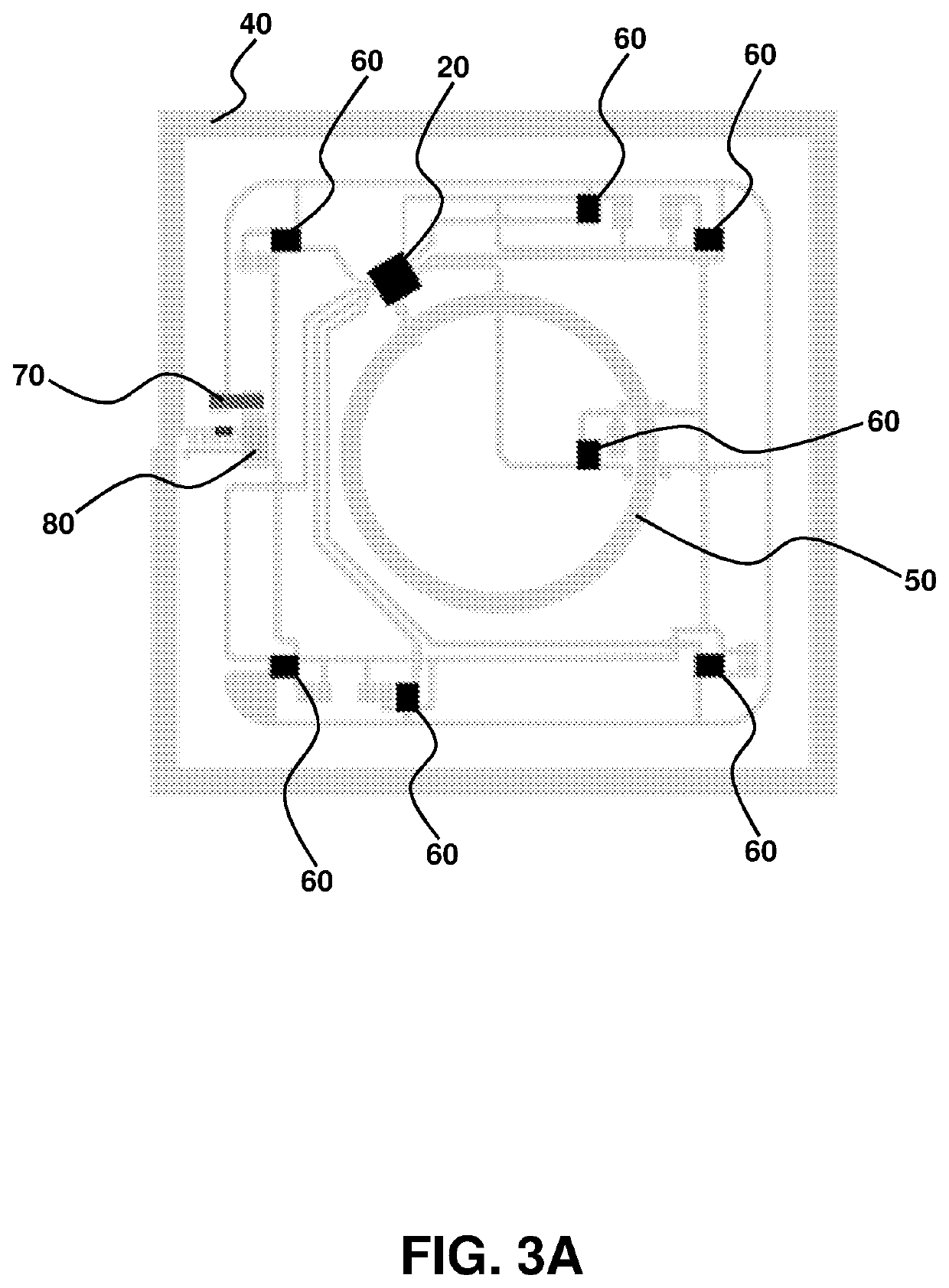
[0106]FIGS. 1-2, 3A and 3B describe a demonstrator actuator device, having a 3″×3″ square footprint with seven independently-controlled actuators spatially separated, in this example in a circular array configuration with one actuator at the origin and the other spatially distributed around the central actuator at the origin. The device is wireless and can be operated without batteries, if desired. Furthermore, the device is readily scaled to have any size footprint, and may be tiled across the body, without limitation. The device has a range of design flexibility, including in size, shape and form factor, and has mechanical characteristics described as soft, flexible and bendable. The devices are readily manufactured.
[0107]FIG. 1 is an actuation device circuit schematic showing a plurality of spatially distributed actuators 10 connected to a wireless controller 20 and a wireless power system 30. The wireless power system may comprise a large area antenna ...
example 2
Characterization of VR Devices
[0127]FIG. 20 illustrates an exemplary VR device. Panel a is an exploded-view schematic illustrations of an epidermal VR device with 32 mechanical actuators. The exploded view assists with visualizing the various components and layers, including the actuators (further illustrated in panels b-f), supported on a soft substrate (labeled as “soft PDMS”) for facilitating comfortable conformal contact with the skin. Other illustrated components include the electronic components, flexible circuit, NFC electronics (further illustrated in panel g with images in panels h and i). Panel b is a schematic illustration of an actuator. Panels c and d are schematic diagrams of an actuator viewing from top (c) and bottom (d). Panels e and f are optical images of an actuator viewing from top (e) and bottom (f). Panel g is a schematic illustration of the NFC electronics with flexible Cu circuit. The inset shows a magnified view of the serpentine shape Cu coil. Panels h and...
PUM
 Abstract
Description
Claims
Application Information


